华工正源中文站华工正源
- +86-27-87180102
-
社交媒体
 微信公众账号
 手机站
手机站
 微信公众账号
 手机站
手机站

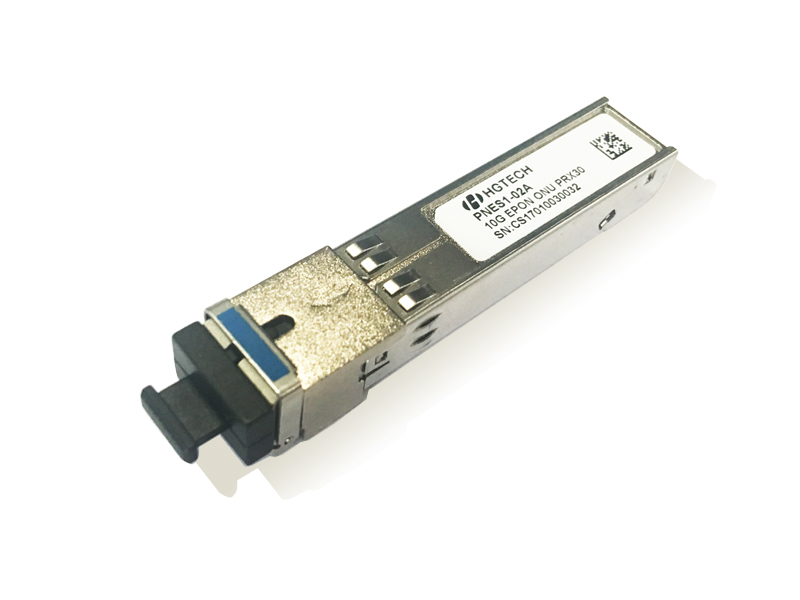
| 产品模块: | 10G EPON ONU PRX30 SFP+ Transceiver |
| 订购信息: | |
| 验证码: |
|
| 类 别: | 电子邮箱: | ||
| 电 话: | QQ: | ||
| *标题: | |||
| *留言内容: | |||
| *验证码: |
|
||
Description
The HG Genuine PNES1-02A transceiver consists 1310nm DFB laser, 1577nm APD photodiode WDM filter and Preamplifier in a high-integrated optical sub-assembly for 1.25G upstream and 10G downstream EPON applications up to 20km. The optical interface is SC/UPC receptacle. It adopts SFP+ Package. Power supply is single +3.3 Voltage.
Features
l SFP+ Package.
l Single Power Supply +3.3 Voltage.
l Sleep Mode compliance
l Single Fiber Bi-Directional SC/UPC receptacle.
l Burst-Mode Transmitter, operation wavelength at 1310nm, 1.25Gbps
l Continuous-Mode Receiver, operation wavelength at 1577nm, 10.3125Gbps
l SFP electrical interface
l 2-wire interface for integrated Digital Diagnostic monitoring
l Operating temperature range: -40 °C ~+85 °C
Applications
l 10 Gigabit PON ONU for P2MP application
Compliance
l Compliant with IEEE 802.3av PRX30
l RoHS compliance
Specification
Absolute Maximum Ratings | ||||||
Parameter | Symbol | Min | Typical | Max | Unit | Notes |
Storage Temperature | TSTG | -40 | 85 | ºC | ||
Operating Relative Humidity | 5 | 95 | % | |||
Supply Voltage | VCC | -0.5 | 4 | V | ||
Recommended Operating Conditions | ||||||
Parameter | Symbol | Min | Typical | Max | Unit | Notes |
Case Operation Temperature | Ta | -40 | 85 | ºC | ||
Supply Voltage | VCC | 3.135 | 3.3 | 3.465 | V | |
Module Power Dissipation | P | 1.3 | W | |||
Tested under recommended operating conditions, unless otherwise noted
Transmitter Operating Characteristic-Optical,Electrical | |||||||
Parameter | Symbol | Min | Typical | Max | Units | Notes | |
Data Rate | BR | 1.25 | Gb/s | ||||
Transmitter differential input voltage | 200 | - | 1600 | mV | |||
Tx burst input | VOH | 2.0 | - | Vcc | V | LVTTL | |
VOL | 0 | - | 0.8 | LVTTL | |||
Tx _SD Voltage | VOH | 2.4 | - | Vcc | V | LVTTL | |
VOL | 0 | - | 0.4 | LVTTL | |||
Center Wavelength | λC | 1260 | 1310 | 1360 | nm | ||
Optical Power Output | BOL | PO | 1.62 | 5.62 | dBm | ||
EOL | 0.62 | 5.62 | |||||
Spectral Width@-20dB | Δλ | 1 | nm | ||||
Side Mode Suppression Ratio | SMSR | 30 | - | - | dB | ||
Extinction Ratio | ER | 6 | dB | ||||
Transmitter and Dispersion Penalty | TDP | - | - | 1.4 | dB | 1 | |
Output Optical Eye | Compliant with IEEE 802.3av | ||||||
Average launch power of OFF transmitter | Poff | -45 | dBm | ||||
Ton | 30 | ns | |||||
Optical Burst Off Time | Toff | 30 | ns | ||||
Tx_indication assert | Tindi-on | 1000 | ns | ||||
Tx_indication deassert | Tindi-off | 1000 | ns | ||||
Receiver OperatingCharacteristic-Optical,Electrical | |||||||
Parameter | Symbol | Min | Typical | Max | Units | Notes | |
Data Rate | BR | 10.3125 | Gb/s | ||||
Receiver differential output voltage | 300 | - | 850 | mV | |||
Rx _LOS Voltage | VOH VOL | 2.4 | - | Vcc | V | LVTTL | |
0 | - | 0.4 | LVTTL | ||||
Sensitivity | BOL | Rx sens | - | - | -29 | dBm | 2 |
EOL | - | - | -28.5 | ||||
Maximum Overload Power | Rx OVERLOAD | -8 | - | - | dBm | ||
Maximum Input Power | Rx max | 0 | dBm | ||||
Input Operating Wavelength | λRX | 1575 | 1577 | 1580 | nm | ||
Optical reflectance | RRX | - | - | -12 | dB | λ=1577nm | |
Rx_LOS Assert | PA | -45 | - | - | dBm | ||
Rx_LOS Deassert | PD | - | - | -29.5 | dBm | ||
Hysteresis | PA - PD | 0.5 | 2.5 | 6 | dB | ||
Notes:
[1]Transmit on 20km SMF.
[2] Measured with PRBS 2^31-1 test pattern @10.3125Gbps with Tx on, ER=8dB, BER=10^-3.
![]()
![]() Digital Diagnostic Memory Map
Digital Diagnostic Memory Map
2 wire address 1010000X (A0) 2 wire address 1010001X (A2)
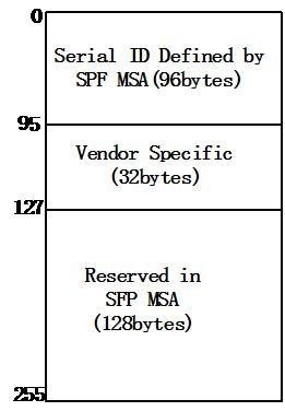
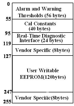
Figure1
EEPROM Serial ID Memory Contents
Accessing Serial ID Memory uses the 2 wire address 1010000X (A0). Memory Contents of Serial ID are shown in Table 1
Table 1 Serial ID Memory Contents
Data Address | Size (Bytes) | Name of Field | Contents(Hex) | Description |
BASE ID FIELDS | ||||
0 | 1 | Identifier | 03 | SFP |
1 | 1 | Ext. Identifier | 04 | SFP function is defined by serial ID only |
2 | 1 | Connector | 01 | SC Connector |
3-10 | 8 | Transceiver | 0x00 0x00 0x00 0x00 0x00 0x00 0x00 0x00 | |
11 | 1 | Encoding | 01 | 8B/10B |
12 | 1 | BR, Nominal | 0D | 1250bps |
13 | 1 | Reserved | 00 | |
14 | 1 | Length (9μm) km | 14 | 20km |
15 | 1 | Length (9μm) 100m | C8 | 20km |
16 | 1 | Length (50μm) 10m | 00 | |
17 | 1 | Length(62.5μm)10m | 00 | |
18 | 1 | Length (Copper) | 00 | Not compliant |
19 | 1 | Reserved | 00 | |
20-35 | 16 | Vendor name | 48 47 20 47 45 4E 55 49 4E 45 20 20 20 20 20 20 | “HG GENUINE” (ASCII) |
36 | 1 | Reserved | 00 | |
37-39 | 3 | Vendor OUI | 00 00 00 | |
40-55 | 16 | Vendor PN | 50 4E 45 53 31 2D 30 32 41 20 20 20 20 20 20 20 | “PNES1-02A” (ASCII) |
56-59 | 4 | Vendor rev | 00 00 00 00 | |
60-61 | 2 | Wavelength | 05 1E | Transceiver wavelength |
62 | 1 | Reserved | 00 | |
63 | 1 | CC_BASE | Check Sum (Variable) | Check code for Base ID Fields |
EXTENDED ID FIELDS | ||||
64-65 | 2 | Options | 00 0C | Soft TX_FAULT,RX_LOS,implemented |
66 | 1 | BR, max | 00 | |
67 | 1 | BR, min | 00 | |
68-83 | 16 | Vendor SN | 30 30 34 39 34 39 30 35 20 20 20 20 20 20 20 20 | Serial Number of transceiver (ASCII). For example “00494905”. |
84-91 | 8 | Date code | 31 36 30 35 30 35 20 20 | Manufactory date code. For example “160505”. |
92 | 1 | Diagnostic Monitoring Type | 68 | Digital diagnostic monitoring implemented, “internally calibrated” is implemented. RX measurement type is “Average Power”. |
93 | 1 | Enhanced Options | B0 | Optional Alarm/Warning flags implemented for all monitored quantities, Optional Soft TX_FAULT monitoring implemented, Optional Soft RX_LOS monitoring implemented. |
94 | 1 | SFF_8472 Compliance | 03 | Includes functionality described in Rev 10.2 SFF-8472. |
95 | 1 | CC_EXT | Check Sum (Variable) | Check sum for Extended ID Field. |
VENDOR SPECIFIC ID FIELDS | ||||
96-127 | 32 | Vendor Specific | Read only | Depends on customer information |
Diagnostic Monitor Functions
Diagnostic Monitor Functions interface uses the 2 wire address 1010001X (A2). Memory contents of Diagnostic Monitor Functions are shown in Table 2.
Table 2 Memory contents of Diagnostic Monitor Function
Data Address | Field Size (bytes) | Name | Contents and Description |
Alarm and Warning Thresholds | |||
00-01 | 2 | Temperature High Alarm | MSB at low address,90℃ |
02-03 | 2 | Temperature Low Alarm | MSB at low address,-45℃ |
04-05 | 2 | Temperature High Warning | MSB at low address,85℃ |
06-07 | 2 | Temperature Low Warning | MSB at low address,- 40℃ |
08-09 | 2 | Vcc High Alarm | MSB at low address,3.63V |
10-11 | 2 | Vcc Low Alarm | MSB at low address,2.97V |
12-13 | 2 | Vcc High Warning | MSB at low address,3.47V |
14-15 | 2 | Vcc Low Warning | MSB at low address,3.13V |
16-17 | 2 | Bias High Alarm | MSB at low address |
18-19 | 2 | Bias Low Alarm | MSB at low address |
20-21 | 2 | Bias High Warning | MSB at low address |
22-23 | 2 | Bias Low Warning | MSB at low address |
24-25 | 2 | TX Power High Alarm | MSB at low address,6.62dBm |
26-27 | 2 | TX Power Low Alarm | MSB at low address,-0.48dBm |
28-29 | 2 | TX Power High Warning | MSB at low address,5.62dBm |
30-31 | 2 | TX Power Low Warning | MSB at low address,0.62dBm |
32-33 | 2 | RX Power High Alarm | MSB at low address,-9.0dBm |
34-35 | 2 | RX Power Low Alarm | MSB at low address,-29.5dBm |
36-37 | 2 | RX Power High Warning | MSB at low address,-10.0dBm |
38-39 | 2 | RX Power Low Warning | MSB at low address, -28.5dBm |
40-55 | 16 | Reserved | |
Calibration Constants | |||
56-59 | 4 | RX Power Calibration Data4 | 00 00 (fixed) |
60-63 | 4 | RX Power Calibration Data3 | 00 00 (fixed) |
64-67 | 4 | RX Power Calibration Data2 | 00 00 (fixed) |
68-71 | 4 | RX Power Calibration Data1 | 00 01 (fixed) |
72-75 | 4 | RX Power Calibration Data0 | 00 00 (fixed) |
76-77 | 2 | Bias Calibration Data1 | 00 01 (fixed) |
78-79 | 2 | Bias Calibration Data0 | 00 00 (fixed) |
80-81 | 2 | TX Power Calibration Data1 | 00 01 (fixed) |
82-83 | 2 | TX Power Calibration Data0 | 00 00 (fixed) |
84-85 | 2 | Temperature Calibration Data1 | 00 01 (fixed) |
86-87 | 2 | Temperature Calibration Data0 | 00 00 (fixed) |
88-89 | 2 | VCC Calibration Data1 | 00 01 (fixed) |
90-91 | 2 | VCC Calibration Data0 | 00 00 (fixed) |
92-94 | 3 | Reserved | 00 00 00 (fixed) |
95 | 1 | Check Sum | Checksum of bytes 0-94 |
Real Time Diagnostic Monitor Interface | |||
96-97 | 2 | Measured Temperature | Yield a 16-bit A/D value (see Table 2.1) |
98-99 | 2 | Measured Vcc | Yield a 16-bit A/D value (see Table 2.1) |
100-101 | 2 | Measured Bias | Yield a 16-bit A/D value (see Table 2.1) |
102-103 | 2 | Measured TX Power | Yield a 16-bit A/D value (see Table 2.1) |
104-105 | 2 | Measured RX Power | Yield a 16-bit A/D value (see Table 2.1) |
106-109 | 4 | Reserved | |
110 | 1 | Logic Status | See Table 2.2 |
111 | 1 | Reserved | |
112-119 | 8 | Alarm and Warning Flags | See Table 2.3 |
Vendor Specific | |||
120-127 | 8 | Vendor Specific | Vendor Specific |
128-247 | 120 | User writable EEPROM | User writable EEPROM |
248-255 | 8 | Vendor Specific | Vendor Specific |
The measured values located at bytes 96-105(in the 2 wire address 0xA2) are raw A/D values (16-bit integers) of transceiver temperature, supply voltage, laser bias current, laser optical output power and received power. All the measured values are “Externally Calibrated”, and then it is necessary to convert raw A/D values to real world units by the manner as shown in Table 2.1.
Table 2.1 Real Time Diagnostic Monitor Values
Byte | Name | Description |
96 | Temperature MSB | Internally measured transceiver temperature. Compliant with External Calibration of SFF-8472. |
97 | Temperature LSB | |
98 | VCC MSB | Internally measured supply voltage. Compliant with External Calibration of SFF-8472. |
99 | VCC LSB | |
100 | Laser Bias MSB | Measured Laser bias current. Compliant with External Calibration of SFF-8472. |
101 | Laser Bias LSB | |
102 | Tx Power MSB | Measured Tx power. Compliant with External Calibration of SFF-8472. |
103 | Tx Power LSB | |
104 | Rx Power MSB | Measured Tx power. Compliant with External Calibration of SFF-8472. |
105 | Rx Power LSB |
This transceiver implements one optional status bytes, “Logic States” at byte 110(0xA2)” as shown in Table 2.2.
Table 2.2 Logic Status and AD Conversion Updates
Byte | Bit | Name | Description |
110 | 7 | Reserved | Reserved |
110 | 6 | Reserved | Reserved |
110 | 5 | Reserved | |
110 | 4 | Reserved | |
110 | 3 | Reserved | Reserved |
110 | 2 | Tx Fault | Optional digital state of the Tx Fault output pin. |
110 | 1 | RX_LOS | Optional digital state of the RX_LOS output pin. |
110 | 0 | Reserved | Reserved |
Each of the measured values has a corresponding high alarm, low alarm, high warning and low warning threshold level at location 00-39(x0A2) written as the data format of a corresponding valued shown in Table 2.3.Alarm and warning flags at bytes 112-119(0xA2) are defined as follows.
[1] Alarm flags indicate conditions likely to result (or have resulted) in link failure and cause for immediate action.
[2] Warning flags indicate conditions outside the guaranteed operating specification of transceiver but not necessarily causes of immediate link failures.
Table 2.3 Alarm and Warning Flags
Byte | Bit(s) | Name | Description |
112 | 7 | Temperature High Alarm | Set when temperature monitor value exceeds high alarm level. |
112 | 6 | Temperature Low Alarm | Set when temperature monitor value exceeds low alarm level. |
112 | 5 | Vcc High Alarm | Set when Vcc monitor value exceeds high alarm level. |
112 | 4 | Vcc Low Alarm | Set when Vcc monitor value exceeds Low alarm level. |
112 | 3 | Laser Bias High Alarm | Set when laser bias monitor value exceeds high alarm level. |
112 | 2 | Laser Bias Low Alarm | Set when laser bias monitor value exceeds low alarm level. |
112 | 1 | Tx Power High Alarm | Set when Tx power monitor value exceeds high alarm level |
112 | 0 | Tx Power Low Alarm | Set when Tx power monitor value exceeds low alarm level. |
113 | 7 | Rx Power High Alarm | Set when Rx power monitor value exceeds high alarm level |
113 | 6 | Rx Power Low Alarm | Set when Rx power monitor value exceeds low alarm level |
113 | 5-0 | Reserved | All bits set to 0. |
114 | 7-0 | Reserved | All bits set to 0. |
115 | 7-0 | Reserved | All bits set to 0. |
116 | 7 | Temperature High warning | Set when temperature monitor value exceeds high warning level. |
116 | 6 | Temperature Low warning | Set when temperature monitor value exceeds low warning level. |
116 | 5 | Vcc High warning | Set when Vcc monitor value exceeds high warning level. |
116 | 4 | Vcc Low warning | Set when Vcc monitor value exceeds Low warning level. |
116 | 3 | Laser Bias High warning | Set when laser bias monitor value exceeds high warning level. |
116 | 2 | Laser Bias Low warning | Set when laser bias monitor value exceeds low warning level. |
116 | 1 | Tx Power High warning | Set when Tx power monitor value exceeds high warning level |
116 | 0 | Tx Power Low warning | Set when Tx power monitor value exceeds low warning level. |
117 | 7 | Rx Power High warning | Set when Rx power monitor value exceeds high warning level |
117 | 6 | Rx Power Low warning | Set when Rx power monitor value exceeds low warning level |
117 | 5-0 | Reserved | All bits set to 0. |
118 | 7-0 | Reserved | All bits set to 0. |
119 | 7-0 | Reserved | All bits set to 0. |
Internal Calibration
Measurements stored in data address byte 96~ 105 are calibrated over transceiver operating temperature and supply voltage and are interpreted as defined in SFF-8472 Rev9.5. Alarm and warning threshold values should be interpreted in the same manner as real time 16 bit data.
External Calibration
Measurements are raw A/D values and must be converted to real world units using calibration constants stored in EEPROM locations 56 – 95 at 2 wire serial bus address A2h. Calibration is valid over transceiver operating temperature and voltage.
Alarm and warning threshold values should be interpreted in the same manner as real time 16 bit data.
After calibration per the equations given below for each variable as described in SFF-8472 Rev9.5, the results are consistent with the accuracy and resolution goals for internally calibrated devices.
Internally measured transceiver temperature. Temperature, T (oC), is given by
T = TSLOPE * TAD + TOFFSET
Where TAD is 16-bit signed 2's complement A/D value at bytes 96-97, TSLOPE is unsigned fixed-point value
at bytes 84-85 and TOFFSET is signed 2's complement value with LSB equal to 1/256 deg-C at bytes 86-87.
The result, T, is 16-bit signed 2's complement value with LSB equal to 1/256 OC, yielding a total range of
-128 OC to +128 OC.
Internally measured supply voltage: Voltage, V (µV), is given by
V = VSLOPE * VAD + VOFFSET
Where VAD is 16-bit unsigned A/D value at bytes 98-99, VSLOPE is unsigned fixed-point value at bytes 88-89 and VOFFSET is signed 2's complement value with LSB equal to 100 µV at bytes 90-91. The result, V, is 16-bit unsigned value with LSB equal to 100 µV, yielding a total range of 0-6.55V.
Measured transmitter laser bias current: Current (µA), I, is given by
I = ISLOPE* IAD + IOFFSET
Where IAD is 16-bit unsigned A/D value at bytes 100-101, ISLOPE is unsigned fixed-point value at bytes
76-77 and IOFFSET is signed 2's complement value with LSB equal to 2 µA at bytes 78-79. The result, I, is
16-bit unsigned value with LSB equal to 2 µA, yielding a total range of 0-131mA.
Measured coupled TX optical output power: Power, TX_P (µW), is given by
TX_P = TX_PSLOPE * TX_PAD + TX_POFFSET
Where TX_PAD is 16-bit unsigned A/D value at bytes 102-103, TX_PSLOPE is unsigned fixed-point value at
bytes 80-81 and TX_POFFSET is signed 2's complement value with LSB equal to 0.1 µW at bytes 82-83. The
result, TX_P, is 16-bit unsigned value with LSB equal to 0.1 µW, yielding a total range of 0-6.5mW.
Measured received optical power: Power, RX_P (µW), is given by
RX_P = R4 * RX_PAD4 + R3 * RX_PAD3 + R2 * RX_PAD2+ R1 * RX_PAD + R0
Where RAD is 16-bit unsigned A/D value at bytes 104-105 and R4, R3, R2, R1 and R0 are single precision
floating-point values at bytes 56-75. The maximum value for R4, R3, R2, R1 and R0 is 1e8. The result,
RX_P, is 16-bit unsigned value with LSB equal to 0.1 µW, yielding a total range of 0-6.5mW.
Digital Diagnostic Monitor Accuracy
Parameter | Range | Actual Value | Calibration Option | Note |
Transceiver Temperature | -40~85℃ | ±3℃ | Internal calibration | Recommended Operating Conditions |
Power Supply Voltage | 3.0-3.6V | ±3% | Internal calibration | Recommended Operating Conditions |
Tx Bias Current | 0~100mA | ±10% | Internal calibration | Recommended Operating Conditions |
Tx BM Optical Power | 0.62~5.62dBm | ±3dB | Internal calibration | Recommended Operating Conditions |
Rx Optical Power | -29~-8dBm | ±3dB | Internal calibration | Recommended Operating Conditions |
Pin-out Description
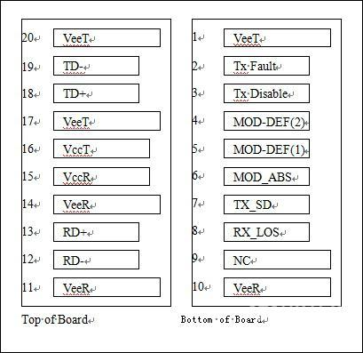
Figure2
Pin Assignment
Pin | Name | Description |
1 | VeeT | Transmitter Ground |
2 | TX Fault | Transmitter Fault Indication |
3 | TX Disable | Transmitter Disable |
4 | MOD-DEF2 | 2 wire serial ID interface, SDA |
5 | MOD-DEF1 | 2 wire serial ID interface, SCL |
6 | MOD_ABS | Module Absent, Grounded in Module |
7 | TX_SD | Tx Transmitter State Indication, TX_Indication Assert When Transmitter ON |
8 | RX_LOS | Loss of Signal |
9 | NC | NC |
10 | VeeR | Receiver Ground |
11 | VeeR | Receiver Ground |
12 | RD- | Inv. Received Data Out.AC couled. |
13 | RD+ | Received Data Out. AC couled. |
14 | VeeR | Receiver Ground |
15 | VccR | Receiver Power |
16 | VccT | Transmitter Power |
17 | VeeT | Transmitter Ground |
18 | TD+ | Transmit Data In. AC-coupled, differential lines with 100Ω differential termination inside the module |
19 | TD- | Inv. Transmit Data In. AC-coupled, differential lines with 100Ω differential termination inside the module |
20 | VeeT | Transmitter Ground |
Function Description
The transceiver provides high-speed Bi-directional serial optical link for EPON 10G downstream and 1.25G upstream application up to 20km.
The burst-mode transmitter part has a 1310 nm DFB laser. It features ac-coupled differential data inputs. TX_BURST is a LVTTL input for TX shut down control. Logic “1” disables the LD driver.
The 1577nm continuous-mode receiver part has a high performance photo detector. The preamplifier (TIA) and limiting amplifier amplify the incoming optical signal into the stable range and convert the signal to differential ac-coupled outputs. RX_LOS is LVTTL output, which logic “1” indicates the input power is lower than the threshold, logic “0” indicates the input power is above the threshold.
Burst Mode Sequence
Tx Burst control: Logic ‘0’ Tx ON
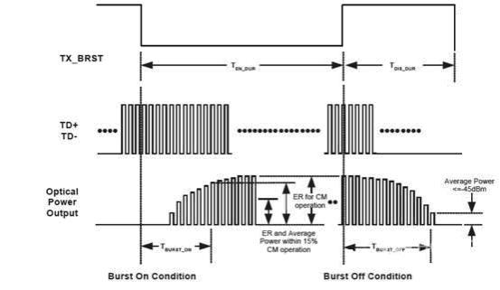
Figure3
Interface Circuit
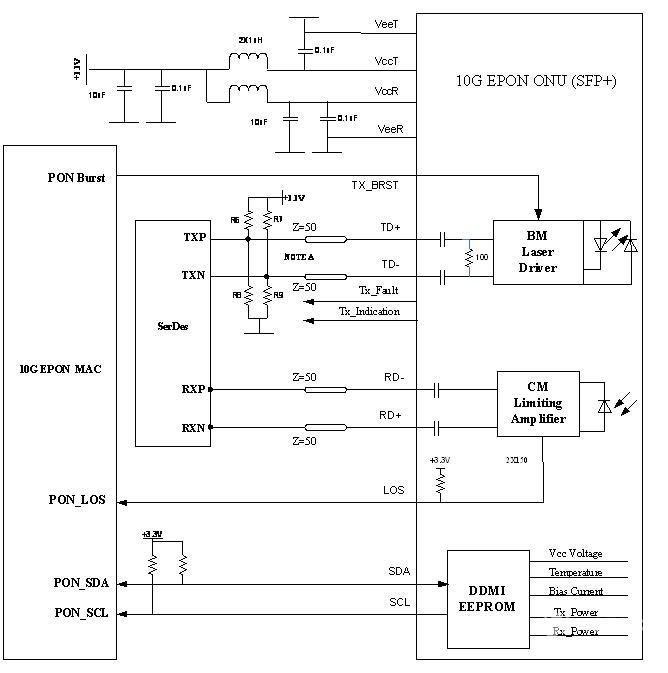
Figure4
Note A: AC coupled internally. R6=R7=N.C, R8=R9=150Ω.
Note B: CML output. AC coupled internally.
Figure Dimensions
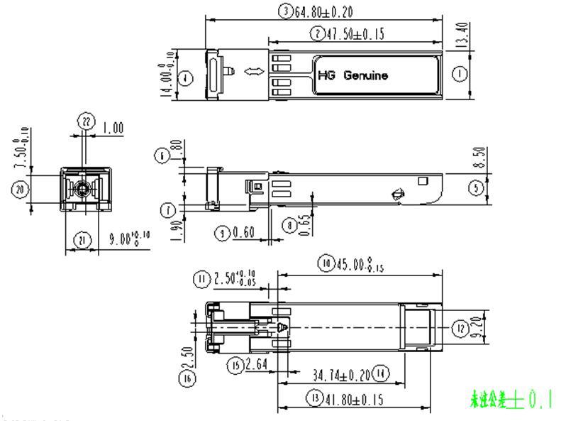
Figure5
Ordering Information
Part No. | Specification | Application | ||||||||
Pack | Rate | Tx | Pout | Rx | S | Top | Reach | Others | ||
PNES1-02A | SFP+ | 1.25Gbps(U) 10.3125Gbs (D) | 1310nm DFB | +0.62~+5.62dBm | APD | <-28.5dBm | -40~85℃ | 20km | “0”Tx ON | PRX30 |
Contact Information
Wuhan Huagong Genuine Optics Technology Co., Ltd
Address: Science & Technology Region of HUST, Donghu High-Tech Zone
Wuhan, Hubei Province, 430223, China
l Tel: +86-27-87180102
l Fax: +86-27-87180220
Email: market@genuine-opto.com
Website: http://www.genuine-opto.com
Statement
HG Genuine possesses the authority for ultimate explanation of all information contained in this document, which is subject to change without prior notice. All the information was obtained in specific environments; and HG Genuine will not be responsible for verifying the products performance in customers’ operating environments, neither liable for the performance of users' products. All information contained is only for the users' reference and shall not be considered as warranted characteristics. HG Genuine will not be liable for damages arising directly or indirectly from any use of the information contained in this document.
Publishing Date: 2015-10-26
Copyright Ó HG Genuine
All Right Reserved