华工正源中文站华工正源
- +86-27-87180102
-
社交媒体
 微信公众账号
 手机站
手机站
微信公众账号
手机站

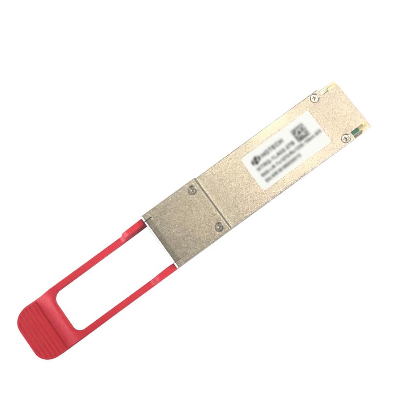
| 产品模块: | 50G QSFP28 ER |
| 订购信息: | |
| 验证码: |
|
| 类 别: | 电子邮箱: | ||
| 电 话: | QQ: | ||
| *标题: | |||
| *留言内容: | |||
| *验证码: |
|
||
Features
Hot-pluggable QSFP28 form factor and Compliant with QSFP+ MSA.
I2C management interface
RoHS-6 compliant (lead-free)
Power dissipation < 3.5W
0°C to 70°C Commercial Temperature Range
Single 3.3V power supply
Maximum link length of 40km on SMF
Optical 26.6GBaud PAM4
IEEE STD 802.3cd Compliant
50GAUI-2 Serial Electrical Interface support
Duplex LC connector
Applications
50G ER applications
Other Optical Links
Standards
Compliant with QSFP+ MSA.
Compliant with SFF-8636
Compliant with IEEE802.3cd
Compliant with IEEE802.3bm
Compliant with RoHS6
Description
The HG Genuine MTRQ-1EA42 QSFP28 transceiver modules is a high performance, cost effective module for 50 Gigabit Ethernet links up to 40km over single mode fiber. They are compliant with the QSFP28 MSA, and IEEE 802.3cd. The Optical transmitter integrated with DSP that translated two lans 26.6GBd NRZ to 26.6GBd PAM4.It contains a single LC connector for the optical interface and a 38-pin connector for the electrical interface. Digital Diagnostics functions are available via a 2-wire serial interface, as specified SFF-8636.
Specifications
Table1-Absolute Maximum Ratings
Parameter | Symbol | Min | Typ. | Max | Unit |
Storage Temperature Range | Ts | -40 | 85 | oC | |
Operating case temperature | Top | -5 | 75 | oC | |
Relative Humidity(non-condensing) | RH | 5 | 85 | % | |
Power Supply Voltage | Vcc | -0.5 | 3.6 | V | |
Receiver Damage Threshold | PT | -2.37 | dBm | ||
ESD Sensitivity | ±500 for High speed lines ±2kV for others | V |
Recommended working conditions
Table2-Recommended Operating Conditions
Parameter | Symbol | Min | Typ. | Max | Unit |
Operating Case Temperature Range | Tc | 0 | - | 70 | oC |
Power Supply Voltage | Vcc | 3.135 | 3.3 | 3.465 | V |
Data Rate(Electrical) | DRe | 26.5625 | Gbps | ||
Data Rate(Optical) | DRo | 53.125 | Gbps | ||
Transmission Distance | 40000 | m |
Optical,Electrical Characteristic
Tested under recommended operating conditions, unless otherwise noted
Table3-Transmitter Operating Characteristic-Optical
Parameter | Symbol | Min. | Typ. | Max. | Unit | Note |
Signaling Rate(range) | 26.5625 ± 100 ppm | GBd | ||||
Wavelengths (range) | WL | 1304.5 | 1317.5 | nm | ||
Module Format | PAM4 | |||||
Average Launch Power | PAVG | 0.4 | 6.63 | dBm | 1 | |
Optical modulation amplitude (OMA) | POMA | 3.4 | 7.4 | dBm | 2 | |
Side-Mode Suppression Ratio | SMSR | 30 | dB | |||
Extinction Ratio | ER | 6 | dB | |||
Launch power in OMA minus TDECQ(min) | 2 | dB | ||||
Transmitter and dispersion eye closure for PAM4 (TDECQ)(max) | 3.2 | dB | ||||
Average launch power of OFF transmitter(max) | -15 | dBm | ||||
RIN OMA(max) | TBD | dB/Hz | ||||
Optical return loss tolerance(max) | TBD | dB | ||||
Transmitter Reflectance(max) | -26 | dB | 3 | |||
Notes:
[1] Min average power is informative and not the principal indicator of signal strength. Power below this value cannot be compliant; however, a value above this does not ensure compliance.
[2] Even if the TDECQ < 1 .4dB, the OMAouter (min) must exceed this value.
[3] Transmitter reflectance is defined looking into the transmitter.
Table4- Receiver Operating Characteristic-Optical
Parameter | Symbol | Min. | Typ. | Max. | Unit | Note |
Signaling rate (range) | 26.5625 ± 100 ppm | GBd | ||||
Modulation format | PAM4 | |||||
Wavelengths (range) | WL | 1304.5 | 1317.5 | nm | ||
Damage threshold | -2.37 | dBm | 1 | |||
Average receive power | -17.6 | -3.37 | dBm | 2 | ||
LOS Assert | LOSA | -30 | dBm | |||
LOS De-Assert | LOSD | -18 | dBm | |||
LOS Hysteresis | 0.5 | dB | ||||
Receiver Sensitivity (OMA) | RS | -15.1 | dBm | 3 | ||
Stressed Receiver Sensitivity (OMA) | RSS | -13.3 | dBm | 4 | ||
Receiver Reflectance | -26 | dB | ||||
Condition of Stressed sensitivity test | ||||||
Stressed Eye Closure | SECQ | 3.2 | dB | 5 | ||
Notes:
[1] The receiver shall be able to tolerate, without damage, continuous exposure to an optical input signal having this average power level
[2] Average receive power (min) is informative and not the principal indicator of signal strength. A received power below this value cannot be compliant; however, a value above this does not ensure compliance.
[3] Receiver sensitivity (OMAouter) (max) is informative and is defined for a transmitter with a value of SECQ up to 3.2 dB for 50GBASE-ER. The value of BER is 2e-4(before FEC).
[4] Measured with conformance test signal at TP3 (see 139.7.10) for the BER specified in 139.1.1 (IEEE802.3cd)
[5] These test conditions are for measuring stressed receiver sensitivity. They are not characteristics of the receiver
Table5- Operating Characteristic- Electrical
Parameter | Symbol | Min. | Typ. | Max. | Unit | Note |
Input Differential Impedance | 100 | Ω | ||||
Differential Data Input Swing | 900 | mV | ||||
Differential Data Output Swing | 900 | mV |
Digital Diagnostic Functions and Control and Status I/O Timing Characteristics
Table6- Digital Diagnostic Functions
Parameter | Symbol | Min | Max | Unit | Notes |
Temperature monitor absolute error | DMI_Temp | -3 | +3 | degC | |
Supply voltage monitor absolute error | DMI _VCC | -5% | 5% | Full operating range | |
Channel RX power monitor absolute error | DMI_RX | -3 | 3 | dB | |
Channel Bias current monitor | DMI_Ibias | -10% | 10% | ||
Channel TX power monitor absolute error | DMI_TX | -3 | 3 | dB |
Table7- Control and Status I/O Timing Characteristics
Parameter | Symbol | Min. | Typ. | Max. | Unit | Note |
Initialization time | t_init | 2000 | ms | 1 | ||
Reset Init Assert Time | t_reset_init | 10 | us | 2 | ||
Serial Bus Hardware Ready Time | t_serial | 2000 | ms | 3 | ||
Reset Assert Time | t_reset | 2000 | ms | 4 | ||
LPMode Assert Time | ton_LPMode | 100 | us | 5 | ||
LPMode Deassert Time | Toff_LPMode | 500 | ms | 6 | ||
IntL Assert Time | ton_IntL | 200 | ms | 7 | ||
IntL Deassert Time | toff_IntL | 500 | us | 8 | ||
Rx LOS Assert Time | ton_los | 100 | ms | 9 | ||
Tx Fault Assert Time | ton_Txfault | 200 | ms | 10 | ||
Flag Assert Time | ton_flag | 200 | ms | 11 | ||
Mask Assert Time | ton_mask | 100 | ms | 12 | ||
Mask Deassert Time | toff_mask | 100 | ms | 13 | ||
Power_override or Power_set Assert Time | ton_Pdown | 100 | ms | 14 | ||
Power_override or Power_set Deassert Time | toff_Pdown | 600 | ms | 15 |
Notes:
[1] Time from power on, hot plug or rising edge of reset until the module is fully functional. This time does not apply to non-Power level 0 modules in Low Power State.
[2] A Reset is generated by a low level longer than t_reset_init present on the ResetL input.
[3] Time from power on until the module responds to data transmission over the two wire serial bus.
[4] Time from assertion of LPMode (Vin:LPMode = Vih) until module power consumption reaches Power Level 1.
[5] Time from deassertion of LPMode (Vin:LPMode = Vil) until module is fully functional,
[6] Time from occurrence of condition triggering IntL until Vout:IntL=Vol.
[7] Time from clear on read operation of associated flag until Vout:IntL=Voh. This includes deassert times for Rx LOS, Tx Fault and other flag bits.
[8] Time from Rx LOS state to Rx LOS bit set (value = 1b) and IntL asserted.
[9] Time from Tx Fault state to Tx Fault bit set (value = 1b) and IntL asserted.
[10] Time from condition triggering flag to associated flag bit set (value = 1b) and IntL asserted.
[11] Time from mask bit set (value = 1b) until associated IntL assertion is inhibited.
[12] Time from mask bit cleared (value = 0b) until associated IntL operation resumes.
[13] Time from change of state of Application or Rate Select bit until transmitter or receiver bandwidth is in conformance with appropriate specification.
[14] Time from P_Down bit set (value = 1b) until module power consumption reaches Power Level 1
[15] Time from P_Down bit cleared (value = 0b) until module is fully functional.
Pin-out Definition

Table8-Pin Function Definitions
Pin | Name | Description | Notes |
1 | GND | Ground | 1 |
2 | Tx2n | Transmitter Inverted Data Input | |
3 | Tx2p | Transmitter Non-Inverted Data Input | |
4 | GND | Ground | 1 |
5 | NC | 3 | |
6 | NC | 3 | |
7 | GND | Ground | |
8 | ModSelL | Module Select | |
9 | ResetL | Module Reset | |
10 | Vcc Rx | +3.3V Power Supply Receiver | 2 |
11 | SCL | 2-wire serial interface clock | |
12 | SDA | 2-wire serial interface data | |
13 | GND | Ground | |
14 | NC | 3 | |
15 | NC | 3 | |
16 | GND | Ground | 1 |
17 | Rx1p | Receiver Non-Inverted Data Output | |
18 | Rx1n | Receiver Inverted Data Output | 1 |
19 | GND | Ground | 1 |
20 | GND | Ground | |
21 | Rx2n | Receiver Inverted Data Output | |
22 | Rx2p | Receiver Non-Inverted Data Output | |
23 | GND | Ground | |
24 | NC | 3 | |
25 | NC | 3 | |
26 | GND | Ground | 1 |
27 | ModPrsL | Module Present | |
28 | IntL | Interrupt | |
29 | VccTx | +3.3V Power supply transmitter | 2 |
30 | Vcc1 | +3.3V Power supply | 2 |
31 | LPMode | Low Power Mode | |
32 | GND | Ground | 1 |
33 | NC | 3 | |
34 | NC | 3 | |
35 | GND | Ground | 1 |
36 | Tx1p | Transmitter Non-Inverted Data Input | |
37 | Tx1n | Transmitter Inverted Data Input | |
38 | GND | Ground | 1 |
Notes:
[1] GND is the symbol for signal and supply (power) common for the QSFP+ module. All are common within the QSFP+ module and all module voltages are referenced to this potential unless otherwise noted. Connect these directly to the host board signal-common ground plane.
[2] Vcc Rx, Vcc1 and VccTx are the receiver and transmitter power supplies and shall be applied concurrently. Recommended host board power supply filtering is shown in Figure 7. Vcc Rx Vcc1 and VccTx may be internally connected within the QSFP+ Module in any combination. The connector pins are each rated for a maximum current of 500 mA.
[3] NC is Not Connect.
Block Diagram of Transceiver

Recommended Interface Circuit
The host board should use the power supply filtering equivalent to that shown in Figure4. Any voltage drop across a filter network on the host is counted against the host DC set point accuracy specification. Inductors with DC resistance of less than 0.1 Ohm should be used in order to maintain the required voltage at the Host Edge Card Connector. It is recommended that the 22 uF capacitors each have an equivalent series resistance of 0.22 ohm.

Mechanical Dimensions
Unit is millimeter.

Digital Diagnostic Memory Map

Table9-EEPROM Serial ID Memory Contents (Upper page 00h) Addr. Field Size Name of Field Hex Description (Bytes) 128 1 Identifer 11 QSFP28 129 1 Ext. Identifier CC Serial ID module 130 1 Connector 07 LC Connector 131-138 8 Transceiver 80 00 00 00 00 00 00 00 139 1 Encoding 08 PAM4 140 1 Nominal Bit Rate FF See Byte 222 141 1 Rate Select 00 Not compliant 142 1 Link Length(Standard SM Fiber) 28 Transceiver transmit distance,40*km 143 1 Link Length(OM3) 00 Not compliant 144 1 Link Length(OM2) 00 Not compliant 145 1 Link Length(OM1) 00 Not compliant 146 1 Link Length(Cooper) 00 Not compliant 147 1 Device Tech 66 1311nm DFB No wavelength control; cooled transmitter device APD detector Transmitter not tuneable 148-163 16 Vendor name 48 47 20 47 45 4E 55 49 4E 45 20 20 20 20 20 20 “HG GENUINE” Vendor Name(ASCII) 164 1 Electronic or optical interfaces for InfiniBand 00 . 165-167 3 Vendor OUI 00 00 00 168-183 16 Vendor PN 4D 54 52 51 2D 31 4C 41 34 32 20 20 20 20 20 20 “MTRQ-1LA42”Part No.(ASCII) 184-185 2 Vendor rev 41 30 186-187 2 Wavelength 66 6C Transceiver wavelength,1311nm 188-189 2 Wavelength Tolerance 05 14 ±6.5nm 190 1 Max Case Temp 46 Max Case Temp 70°C 191 1 Check Sum 63 Address 128-190 Checksum 192-195 4 Rate Select,TX Disable,TX Fault,LOS,Warming indicators 00 08 00 98 196-211 16 Vendor SN SN(Variable) Serial Number of transceiver(ASCII). 212-219 8 Date code DC(Variable) Manufactory Date Code. 220 1 Diagnostic Monitoring Type 0C Average Power 221 1 Enhanced Options 10 222 1 Extended bit rate D5 Nominal bit rate per lane, units of 250 Mbps - 223 1 Check Sum (Variable) Address 192-222 224-255 Reserved Read only Filled by zero Table10-EEPROM DDM Alarm & Warning Threshold (Upper page 03h) Addr. Field Size Name of Field Hex Description (Bytes) 128-129 2 Temperature High Alarm 50 00 80℃ 130-131 2 Temperature Low Alarm F6 00 -10℃ 132-133 2 Temperature High Warning 46 00 70℃ 134-135 2 Temperature Low Warning 00 00 0℃ 144-145 2 Vcc High Alarm 8D CC 3.63V 146-147 2 Vcc Low Alarm 74 04 2.97V 148-149 2 Vcc High Warning 87 5A 3.465V 150-151 2 Vcc Low Warning 7A 76 3.135V 176-177 2 RX Power High Alarm 27 10 0dBm 178-179 2 RX Power Low Alarm 00 9E -18dBm 180-181 2 RX Power High Warning 13 88 -3dBm 182-183 2 RX Power Low Warning 01 3C -15dBm 184-185 2 Bias High Alarm FF FF 131mA 186-187 2 Bias Low Alarm 09 C4 5mA 188-189 2 Bias High Warning FD E8 130mA 190-191 2 Bias Low Warning 13 88 10mA 192-193 2 TX Power High Alarm FF FF 8.16dBm 194-195 2 TX Power Low Alarm 1B A8 -1.5dBm 196-197 2 TX Power High Warning F6 78 8.0dBm 198-199 2 TX Power Low Warning 37 2D 1.5dBm Ordering Information Table11- Ordering Information Part No Specification Pack Rate Tx Pout Rx S Top Reach Others MTRQ-1EA42 QSFP28 50G DFB/EML 0.4~6.63 dBm APD <-15.1 dBm 0~70℃ 40KM DDM/RoHS Contact Information Wuhan Huagong Genuine Optics Technology Co., Ltd Address: Science & Technology Region of HUST, Donghu High-Tech Zone Wuhan, Hubei Province, 430223, China Tel: +86-27-87180102 Fax: +86-27-87180220 Email: market@genuine-opto.com Website: http://www.genuine-opto.com Statement HG Genuine possesses the authority for ultimate explanation of all information contained in this document, which is subject to change without prior notice. All the information was obtained in specific environments; and HG Genuine will not be responsible for verifying the products performance in customers’ operating environments, neither liable for the performance of users' products. All information contained is only for the users' reference and shall not be considered as warranted characteristics. HG Genuine will not be liable for damages arising directly or indirectly from any use of the information contained in this document. Publishing Date: 18 Feb,2019 Copyright Ó HG Genuine All Right Reserved
