华工正源中文站华工正源
- +86-27-87180102
-
社交媒体
 微信公众账号
 手机站
手机站
微信公众账号
手机站

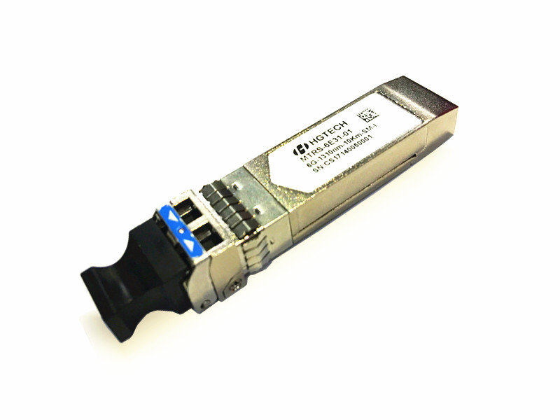
| 产品模块: | 6G 10km SFP+ Transceiver |
| 订购信息: | |
| 验证码: |
|
| 类 别: | 电子邮箱: | ||
| 电 话: | QQ: | ||
| *标题: | |||
| *留言内容: | |||
| *验证码: |
|
||
Description
The optical output can be disabled by LVTTL logic high-level input of TX_DIS. Transmit Fault (Tx_Fault) is provided to indicate that the module transmitter has detected a fault condition related to laser operation or safety. Loss of signal (RX_LOS) output is provided to indicate the loss of an input optical signal of receiver. A serial EEPROM in the transceiver allows the user to access transceiver monitoring and configuration data via the 2-wire SFP Management Interface. This interface uses a single address, A0h, with a memory map divided into a lower and upper area. Basic digital diagnostic (DD) data is held in the lower area while specific data is held in a series of tables in the high memory area.
l Up to
l Support Multi Rate 1.25-6.25Gbps
l 1310nm DFB and PIN receiver
l SFI electrical interface
l 2-wire interface for integrated Digital Diagnostic monitoring
l SFP+ MSA package with duplex LC connector
l Hot pluggable
l Very low EMI and excellent ESD protection
l +3.3V power supply
l Power consumption less than 1W
l Operating case temperature: -40~+
l High-speed storage area networks
l Computer cluster cross-connect
l Custom high-speed data pipes
l LTE optical repeater application
l Compliant with Fiber Channel(FC)-Standard INCITS 352
l Compliant with IEEE 802.3ae-2002
l Compliant with FCC 47 CFR Part 15, Class B
l Compliant with FDA 21 CFR 1040.10 and 1040.11, Class I except for deviations pursuant
Specification
Transmitter Operating Characteristic-Optical, Electrical |
|||||||
|
Parameter |
Symbol |
Min. |
Typical |
Max. |
Unit |
Note
|
|
|
Centre Wavelength |
λC |
1260 |
1310 |
1355 |
nm |
Note1 |
|
|
Side Mode Suppression Ratio |
SMSR |
35 |
- |
|
dBm |
|
|
|
Laser Off Power |
Poff |
- |
- |
-30 |
dBm |
|
|
|
Average Optical Power |
Pavg |
-8.2 |
- |
0.5 |
dBm |
Note1 |
|
|
Extinction Ratio |
ER |
3.5 |
- |
- |
dB |
|
|
|
Transmitter Dispersion Penalty |
TDP |
- |
- |
3.2 |
dB |
|
|
|
Relative Intensity Noise |
Rin |
- |
- |
-128 |
dB/Hz |
|
|
|
Optical Return Loss Tolerance |
|
12 |
- |
- |
dB |
|
|
|
Operating Data Rate |
|
- |
- |
6.25 |
Gbps |
|
|
|
Optical Eye Mask |
Compliant with IEEE 802.3ae |
Note2 |
|||||
|
Single Ended Output Voltage Tolerance |
|
-0.3 |
- |
4 |
V |
|
|
|
Common mode voltage tolerance |
|
15 |
- |
- |
mV |
|
|
|
Tx Input Diff Voltage |
VI |
180 |
- |
700 |
mV |
|
|
|
Tx Fault |
VoL |
-0.3 |
- |
0.4 |
V |
At 0.7mA |
|
|
Data Dependent Input Jitter |
DDJ |
- |
- |
0.1 |
UI |
|
|
|
Data Input Total Jitter |
TJ |
- |
- |
0.28 |
UI |
|
|
Notes:
[1] Average optical power shall be measured using the methods specified in TIA/EIA-455-95.
[2] Vertical eye closure penalty and stressed eye jitter are the test conditions for measuring stressed receiver sensitivity. They are not the required characteristic of the receiver.
|
Receiver Operating Characteristic-Optical, Electrical |
||||||
|
Parameter |
Symbol |
Min. |
Typ. |
Max. |
Unit |
Note
|
|
Center Wavelength |
λr |
1260 |
1310 |
1355 |
nm |
|
|
Receiver Sensitivity |
Psens |
- |
- |
-14.4 |
dBm |
|
|
Stressed Sensitivity (OMA) |
|
- |
- |
-12.6 |
dBm |
|
|
LOS Assert |
LosA |
-30 |
- |
- |
dBm |
|
|
LOS Dessert |
LosD |
- |
- |
-16 |
dBm |
|
|
LOS Hysteresis |
LosH |
0.5 |
- |
- |
dB |
|
|
Overload |
Pin |
0.5 |
- |
- |
dBm |
|
|
Stressed Eye Jitter |
|
0.3 |
- |
- |
UIp-p |
Note1 |
|
Receive electrical 3dB upper cutoff frequency |
|
- |
- |
12.3 |
GHz |
|
|
Vertical Eye Closure Penalty |
|
2.2 |
- |
- |
dB |
Note2 |
|
Receiver Reflectance |
|
- |
- |
-12 |
dB |
|
|
Operating Data Rate |
|
- |
- |
6.25 |
Gbps |
|
|
Single Ended Output Voltage Tolerance |
|
-0.3 |
- |
4 |
V |
|
|
Rx Output Diff Voltage |
Vo |
550 |
- |
850 |
mV |
|
|
Rx Output Rise and Fall Time |
Tr/Tf |
30 |
- |
- |
ps |
20% to 80% |
|
Total Jitter |
TJ |
- |
- |
0.7 |
UI |
|
|
Deterministic Jitter |
DJ |
- |
- |
0.42 |
UI |
|
Notes:
[1] Receiver sensitivity is informative. Stressed receiver sensitivity shall be measured with conformance test signal for BER =1x 10-12 .
[2] Vertical eye closure penalty and stressed eye jitter are the test conditions for measuring stressed receiver sensitivity. They are not the required characteristic of the receiver.
|
Control and Status I/O Timing Characteristics |
||||||
|
Parameter |
Symbol |
Min. |
Max. |
Unit |
Note
|
|
|
TX Disable Assert Time |
t_off |
|
10 |
µs |
Note1 |
|
|
TX Disable Negate Time |
t_on |
|
1 |
ms |
Note2 |
|
|
Time to initialize including reset of TX_Fault |
t_init |
|
300 |
ms |
Note3 |
|
|
TX Fault Assert Time |
t_fault |
|
100 |
µs |
Note4 |
|
|
TX Disable to reset |
t_reset |
10 |
|
µs |
Note5 |
|
|
LOS Assert Time |
t_loss_on |
|
100 |
µs |
Note6 |
|
|
LOS Deassert Time |
t_loss_off |
|
100 |
µs |
Note7 |
|
|
Rate-Select Change Time |
t_ratesel |
|
10 |
µs |
Note8 |
|
|
Serial ID Clock Rate |
f_serial_clock |
|
100 |
kHz |
|
|
Notes:
[1] Time from rising edge of TX Disable to when the optical output falls below 10% of nominal
[2] Time from falling edge of TX Disable to when the modulated optical output rises above 90% of nominal
[3] From power on or negation of TX Fault using TX Disable
[4] Time from fault to TX fault on
[5] Time TX Disable must be held high to reset TX_fault
[6] Time from LOS state to RX LOS assert
[7] Time from non-LOS state to RX LOS deassert.
[8] Time from rising or falling edge of Rate Select input until receiver bandwidth is in conformance with appropriate specification
|
Optical Characteristics(Multi Rate Characteristics) |
|||
|
Parameters |
|
|
|
|
Total Power Consumption |
<1W |
<1W |
<1W |
|
Tx Light Output Power |
>-8.2 |
>-8.2 |
>-8.2 |
|
Extinction Ratio |
>3.5 |
>3.5 |
>3.5 |
|
Eye Mask Margin |
>20% |
>20% |
>20% |
|
Rx Sensitivity |
<-22.0dBm |
<-20.0dBm |
<-17.0dBm |
|
Working Temperature |
-40~+ |
-40~+ |
-40~+ |
Notes:
[1] For
