华工正源中文站华工正源
- +86-27-87180102
-
社交媒体
 微信公众账号
 手机站
手机站
微信公众账号
手机站

| 产品模块: | 25G 850nm 0.07km MM SFP28 Transceiver |
| 订购信息: | |
| 验证码: |
|
| 类 别: | 电子邮箱: | ||
| 电 话: | QQ: | ||
| *标题: | |||
| *留言内容: | |||
| *验证码: |
|
||
Description
MTRA-3A90A transceiver is a high performance, cost effective modules, which is optimized for 32G Fibre Channel and 25G Ethernet, supporting MAX data-rate of 28.05Gbps, and transmission distance up to 70m on OM3 MMF.The transceiver consists of two sections: The transmitter section incorporates an 25G 850nm VCSEL, driver and CDR.. The receiver section consists of a PIN photodiode integrated with a transimpedance preamplifier (TIA),limiting amplifier and CDR. The transceiver is hot pluggable into the 20-pin connector .
The high-speed electrical interface is base on low voltage logic, with nominal 100 Ohms differential impedance and AC coupled in the transceiver. The optical output can be disabled by LVTTL logic high-level input of TX_DIS. Loss of signal (RX_LOS) output is provided to indicate the loss of an input optical signal of receiver.
A serial EEPROM in the transceiver allows the user to access transceiver monitoring and configuration data via the 2-wire SFP Management Interface. This interface uses a single address, A0h, with a memory map divided into a lower and upper area. Basic digital diagnostic data is held in the lower area while specific data is held in a series of tables in the high memory area
Features
l Support Data Rate 25Gbps
l Built-in CDR
l Up to 70m transmission distance on OM3 MMF
l 850nm VCSEL and PIN receiver
l SFI electrical interface
l 2-wire interface for integrated Digital Diagnostic monitoring
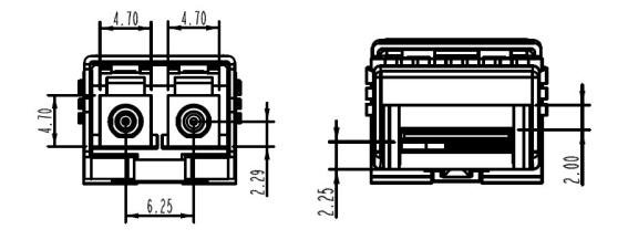
l SFP+ MSA package with duplex LC connector
l Hot pluggable
l Very low EMI and excellent ESD protection
l +3.3V power supply
l Power consumption less than 1W
l Operating case temperature: 0~+70°C
Applications
l 32G Fibre Channel
l 25G BASE-SR
Compliance
l Compliant with SFF-8431
l Compliant with FC-PI-6
l Compliant with FDA 21 CFR 1040.10 and 1040.11, Class I except for deviations pursuant
l RoHS compliance
Specification
|
|
|
|
|
|
|
Parameter |
Symbol |
Min. |
Max. |
Unit |
|
Storage Temperature |
TS |
-40 |
+85 |
℃ |
|
Supply Voltage |
VCC3 |
0 |
3.6 |
V |
|
Relative Humidity(Non-condensing) |
RH |
5 |
85 |
% |
|
RX Input Average Power |
Pmax |
- |
3.4 |
dBm |
|
Recommended Operating Conditions |
|
|
|
|
|
|
Parameter |
Symbol |
Min. |
Typical |
Max. |
Unit |
|
Operating Case Temperature |
TC |
0 |
|
70 |
℃ |
|
Power Supply Voltage |
VCC3 |
3.13 |
3.3 |
3.47 |
V |
|
ICC3 |
|
|
288 |
mA |
|
|
Power Dissipation |
PD |
|
|
1 |
W |
|
Data Rate |
|
|
25.78125 |
|
Gbps |
|
Transmission Distance(OM3 MMF) |
|
|
|
70 |
m |
|
Transmitter Operating Characteristic-Optical, Electrical |
|
|
|
|||
|
Parameter |
Symbol |
Min. |
Typical |
Max. |
Unit |
Note |
|
Center Wavelength |
λC |
840 |
850 |
860 |
nm |
|
|
RMS Spectral Width |
|
|
|
0.6 |
nm |
|
|
Laser Off Power |
Poff |
- |
- |
-30 |
dBm |
|
|
Average Optical Power |
Pavg |
-8.4 |
- |
2.4 |
dBm |
|
|
Optical Modulation Amplitude |
OMA |
-6.4 |
|
3 |
dBm |
|
|
Extinction Ratio |
ER |
2 |
- |
- |
dB |
|
|
Transmitter Dispersion Penalty |
TDP |
- |
- |
4.3 |
dB |
|
|
Optical Return Loss Tolerance |
|
- |
- |
12 |
dB |
|
|
Optical Eye Mask |
|
5 |
|
|
% |
|
|
Differential input impedance |
|
|
100 |
|
Ω |
|
|
Tx Input Diff Voltage |
VI |
180 |
|
700 |
mV |
|
|
Tx Fault |
VoL |
-0.3 |
|
0.4 |
V |
At 0.7mA |
|
IoH |
-50 |
|
37.5 |
uA |
Note1 |
|
|
Tx_Disable |
VIL |
-0.3 |
|
0.8 |
V |
|
|
VIH |
2 |
|
VCC+0.3 |
V |
|
|
Notes:
[1] Measured with a 4.7 kΩ load pulled up to Vcc.
|
Receiver Operating Characteristic-Optical, Electrical |
|
|
|
|||
|
Parameter |
Symbol |
Min. |
Typ. |
Max. |
Unit |
Note |
|
Center Wavelength |
λr |
840 |
850 |
860 |
nm |
|
|
Receiver Sensitivity (Average Power) |
Psens |
|
|
-10.3 |
dBm |
Note1 |
|
Los Assert |
LosA |
-30 |
|
- |
dBm |
|
|
Los Dessert |
LosD |
|
|
-13 |
dBm |
|
|
Los Hysteresis |
LosH |
0.5 |
|
- |
dB |
|
|
Overload |
Pin |
2.4 |
|
|
dBm |
|
|
Receiver Reflectance |
|
|
|
-12 |
dB |
|
|
Rx Output Diff Voltage |
Vo |
300 |
|
900 |
mV |
|
|
Rx_LOS |
VoL |
-0.3 |
|
0.4 |
V |
At 0.7mA |
|
IoH |
-50 |
|
37.5 |
uA |
Note2 |
|
|
RS0,RS1 |
VIL |
-0.3 |
|
0.8 |
V |
|
|
VIH |
2 |
|
VCC+0.3 |
V |
|
|
Notes:
[1] Receiver sensitivity is informative. shall be measured with conformance test signal for BER =5x 10⁻⁵ .
[2] Measured with a 4.7 kΩ load pulled up to Vcc.
|
Control and Status I/O Timing Characteristics |
|
|
|
|
|
|
Parameter |
Symbol |
Min. |
Max. |
Unit |
Note |
|
TX Disable Assert Time |
t_off |
|
100 |
µs |
Note1 |
|
TX Disable Negate Time |
t_on |
|
2 |
ms |
Note2 |
|
Time to initialize including reset of TX_Fault |
t_init |
|
300 |
ms |
Note3 |
|
TX Fault Assert Time |
t_fault |
|
1 |
ms |
Note4 |
|
Tx_Fault Reset |
t_reset |
10 |
|
µs |
Note5 |
|
LOS Assert Time |
t_loss_on |
|
100 |
µs |
Note6 |
|
LOS Deassert Time |
t_loss_off |
|
100 |
µs |
Note7 |
|
Serial ID Clock Rate |
f_serial_clock |
|
400 |
kHz |
|
Notes:
[1] Time from rising edge of TX Disable to when the optical output falls below 10% of nominal
[2] Time from falling edge of TX Disable to when the modulated optical output rises above 90% of nominal
[3] From power on or negation of TX Fault using TX Disable
[4] Time from fault to TX fault on
[5] Time TX Disable must be held high to reset TX_fault
[6] Time from LOS state to RX LOS assert
[7] Time from non-LOS state to RX LOS deassert.
Pin-out Definition
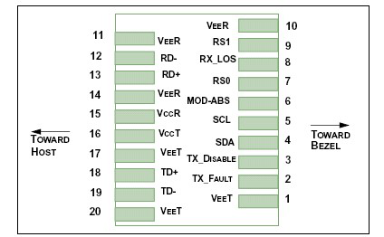
|
Pin |
Logic |
Symbol |
Name/Description |
Note |
|
1 |
|
VeeT |
Module Transmitter Ground |
Note1 |
|
2 |
LVTTL-O |
TX_Fault |
Module Transmitter Fault |
Note2 |
|
3 |
LVTTL-I |
TX_Disable |
Transmitter Disable; Turns off transmitter laser output |
Note3 |
|
4 |
LVTTL-I/O |
SDA |
2-wire Serial Interface Data Line (Same as MOD-DEF2 as defined in the INF-8074i) |
Note4 |
|
5 |
LVTTL-I/O |
SCL |
2-wire Serial Interface Clock (Same as MOD-DEF1 as defined in the INF-8074i) |
Note4 |
|
6 |
|
MOD_ABS |
Module Absent, connected to VeeT or VeeR in the module |
Note5 |
|
7 |
LVTTL-I |
RS0 |
|
Note6 |
|
8 |
LVTTL-O |
RX_LOS |
Receiver Loss of Signal Indication (In FC designated as RX_LOS, in SONET designated as LOS, and in Ethernet designated at Signal Detect) |
Note2 |
|
9 |
LVTTL-I |
RS1 |
. |
|
|
10 |
|
VeeR |
Module Receiver Ground |
Note1 |
|
11 |
|
VeeR |
Module Receiver Ground |
Note1 |
|
12 |
CML-O |
RD- |
Receiver Inverted Data Output |
|
|
13 |
CML-O |
RD+ |
Receiver Non-Inverted Data Output |
|
|
14 |
|
VeeR |
Module Receiver Ground |
Note1 |
|
15 |
|
VccR |
Module Receiver 3.3 V Supply |
|
|
16 |
|
VccT |
Module Transmitter 3.3 V Supply |
|
|
17 |
|
VeeT |
Module Transmitter Ground |
Note1 |
|
18 |
CML-I |
TD+ |
Transmitter Non-Inverted Data Input |
|
|
19 |
CML-I |
TD- |
Transmitter Inverted Data Input |
|
|
20 |
|
VeeT |
Module Transmitter Ground |
Note1 |
Notes:
[1] The module signal ground pins, VeeR and VeeT, shall be isolated from the module case.
[2] This pin is an open collector/drain output pin and shall be pulled up with 4.7k-10kohms to Host_Vcc on the host board. Pull ups can be connected to multiple power supplies, however the host board design shall ensure that no module pin has voltage exceeding module VccT/R + 0.5 V.
[3] This pin is an open collector/drain input pin and shall be pulled up with 4.7k-10kohms to VccT in the module.
[4] See sff-8431 4.2 2-wire Electrical Specifications .
[5] This pin shall be pulled up with 4.7k-10kohms to Host_Vcc on the host board.
Block Diagram of Transceiver
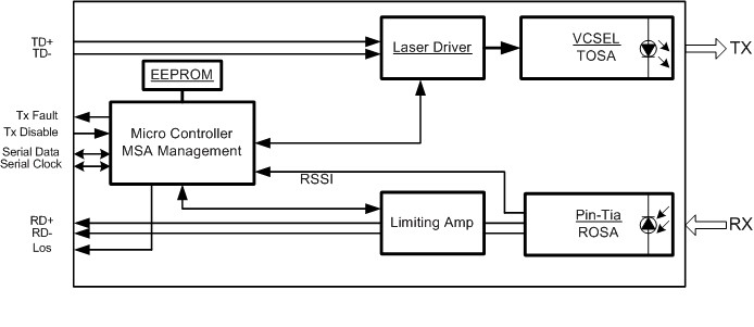
Figure2
The transmitter converts 25Gbit/s serial PECL or CML electrical data into serial optical data compliant with the 32GFC and 25G Ethernet. An open collector compatible Transmit Disable (Tx_Dis) is provided. A logic “1,” or no connection on this pin will disable the laser from transmitting. A logic “0” on this pin provides normal operation. The transmitter has an internal automatic power control loop (APC) to ensure constant optical power output across supply voltage and temperature variations. An open collector compatible Transmit Fault (Tx_Fault) is provided.
TX_Fault is a module output contact that when high, indicates that the module transmitter has detected a fault condition related to laser operation or safety. The TX_Fault output contact is an open drain/collector and shall be pulled up to the Vcc_Host in the host with a resistor in the range 4.7-10 kΩ. TX_Disable is a module input contact. When TX_Disable is asserted high or left open, the SFP+ module transmitter output shall be turned off. This contact shall be pulled up to VccT with a 4.7 kΩ to 10 kΩ resistor
The receiver converts 25Gbit/s serial optical data into serial PECL/CML electrical data. An open collector compatible Loss of Signal is provided. Rx_LOS when high indicates an optical signal level below that specified in the relevant standard. The Rx_LOS contact is an open drain/collector output and shall be pulled up to Vcc_Host in the host with a resistor in the range 4.7-10 kΩ, or with an active termination. Power supply filtering is recommended for both the transmitter and receiver. The Rx_LOS signal is intended as a preliminary indication to the system in which the SFP+ is installed that the received signal strength is below the specified range. Such an indication typically points to non-installed cables, broken cables, or a disabled, failing or a powered off transmitter at the far end of the cable.
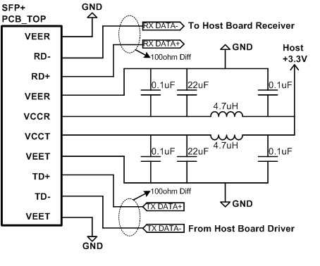
Recommended Interface Circuit

EEPROM Information (A0h)
|
Addr. |
Field Size |
Name of Field |
Hex |
Description |
|||||
|
(Bytes) |
|||||||||
|
0 |
1 |
Identifer |
03 |
SFP28 |
|||||
|
1 |
1 |
Ext. Identifier |
04 |
SFP function is defined by serial ID only |
|||||
|
2 |
1 |
Connector |
07 |
LC Connector |
|||||
|
3-10 |
8 |
Transceiver |
00 00 00 00 00 00 00 00 |
Transceiver Codes |
|||||
|
11 |
1 |
Encoding |
03 |
NRZ |
|||||
|
12 |
1 |
BR, Nominal |
FF |
>25Gb/s |
|||||
|
13 |
1 |
Rate Identifier |
00 |
Unspecified |
|||||
|
14 |
1 |
Length (9um) km |
00 |
Transceiver transmit distance |
|||||
|
15 |
1 |
Length (9um) 100m |
00 |
Transceiver transmit distance |
|||||
|
16 |
1 |
Length (50um)10m |
00 |
OM2 transmit distance,150m |
|||||
|
17 |
1 |
Length (62.5um) 10m |
00 |
Transceiver transmit distance |
|||||
|
18 |
1 |
Length (Copper or OM4) |
0A |
OM4 transmit distance,100m |
|||||
|
19 |
1 |
Length (50um OM3) |
07 |
OM3 transmit distance,70m |
|||||
|
20-35 |
16 |
Vendor name |
48 47 20 47 45 4E 55 49 4E 45 20 20 20 20 20 20 |
“HG GENUINE” Vendor Name(ASCII) |
|||||
|
36 |
1 |
Transceiver |
02 |
25G BASE-SR |
|||||
|
37-39 |
3 |
Vendor OUI |
00 00 00 |
Unspecified |
|||||
|
40-55 |
16 |
Vendor PN |
4D 54 52 41 2D 33 41 39 30 41 20 20 20 20 20 20 |
“MTRA-3A90A”Part No.(ASCII) |
|||||
|
56-59 |
4 |
Vendor rev |
31 2E 30 20 |
“1.0” (ASCII) |
|||||
|
60-61 |
2 |
Wavelength |
03 52 |
Transceiver wavelength |
|||||
|
62 |
1 |
Reserved |
00 |
|
|||||
|
63 |
1 |
CC_BASE |
E0 |
Check code for Base ID Fields |
|||||
|
64-65 |
2 |
Options |
18 1A |
TX_DISABLE, TX_FAULT and Loss of Signal implemented. |
|||||
|
66 |
1 |
BR,MAX |
00 |
Unspecified |
|||||
|
67 |
1 |
BR,MIN |
00 |
Unspecified |
|||||
|
68-83 |
16 |
Vendor SN |
SN(Variable) |
Serial Number of transceiver(ASCII). |
|||||
|
84-91 |
8 |
Date code |
DC(Variable) |
Manufactory Date Code. |
|||||
|
92 |
1 |
Diagnostic Monitoring Type |
68 |
Digital diagnostic monitoring implemented, “Internally calibrated” is implemented |
|||||
|
93 |
1 |
Enhanced Options |
F0 |
Optional Alarm/Warning flags implemented for all monitored quantities, Optional Soft TX_Disable control and monitoring implemented, Optional Soft TX_FAULT monitoring implemented, Optional Soft RX_LOS monitoring implemented |
|||||
|
94 |
1 |
SFF_8472 Compliance |
08 |
Includes functionality described in Rev12.0 SFF-8472 |
|||||
|
95 |
1 |
CC_EXT |
CS(Variable) |
Check sum for Extended ID Field. |
|||||
|
96-127 |
32 |
Vendor Specific |
Read only |
Depends on customer information Filled by zero |
|||||
|
Part No |
|
|
|
Specification |
|
|
|
||
|
Pack |
Rate |
Tx |
Pout |
Rx |
S |
Top |
Reach |
Others |
|
|
MTRA-3A90A |
SFP+ |
25G |
850nm VCSEL |
-8.4 ~ 2.4dBm |
PIN |
<-10.3dBm |
0~70℃ |
70m |
DDM/RoHS |
Contact Information
Wuhan Huagong Genuine Optics Technology Co., Ltd
Address: Science & Technology Region of HUST, Donghu High-Tech Zone
Wuhan, Hubei Province, 430223, China
l Tel: +86-27-87180102
l Fax: +86-27-87180220
Email: market@genuine-opto.com
Statement
HG Genuine possesses the authority for ultimate explanation of all information contained in this document, which is subject to change without prior notice. All the information was obtained in specific environments; and HG Genuine will not be responsible for verifying the products performance in customers’ operating environments, neither liable for the performance of users' products. All information contained is only for the users' reference and shall not be considered as warranted characteristics. HG Genuine will not be liable for damages arising directly or indirectly from any use of the information contained in this document.
Publishing Date: 2016-3-14
Copyright Ó HG Genuine
All Right Reserved
