
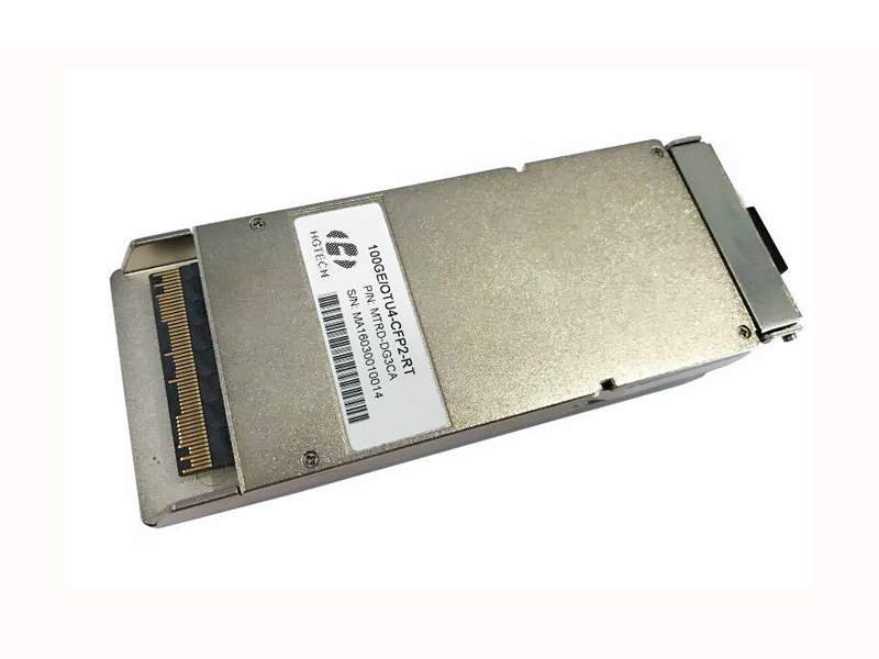
| 产品模块: | 100G BASE-LR4/OTU4 10km CFP2 Transceiver |
| 订购信息: | |
| 验证码: |
|
| 类 别: | 电子邮箱: | ||
| 电 话: | QQ: | ||
| *标题: | |||
| *留言内容: | |||
| *验证码: |
|
||
Description
MTRD-DG3CA CFP2 transceivers are designedfor use in 100Gigabit Ethernet links and OTU4over 10km single module fiber, and it compliant tothe CFP MSA CFP2 HW Specification and IEEE802.3ba 100GBASE-LR4. Digital diagnostics areavailable via MDIO as specified in the CFP MSAManagement Interface Specification.The transceiver's designs are optimized for highperformance and cost efficiency to providecustomers the best solutions for Datacom andTelecom applications.
l Up to10km transmission on SMF
l Support Dual Rate 103.1G and 111.8Gbps
l Transmitter:4-lane*28Gb/s LAN-WDM EML TOSA (1295.56nm,1300.05nm,1304.58nm,1309.14nm)
l Receiver:4-lane*28Gb/s PIN ROSA
l MDIO management interface with Digital Diagnostic
l CFP2 MSA package with duplex LC connector
l +3.3V power supply
l Power consumption less than 9W
l Operating case temperature: 0~+70°C
l 100GE Routers and Switches
l 100G DWDM/OTN
l 100G Network Security
Compliance
l Compliant with IEEE 802.3ba 100GBASER-LR4
l Compliant with ITU-T 411-9D1F
l Compliant with CFP MSA CFP2 Hardware Specification
| Absolute Maximum Ratings |
|
| ||
Parameter | Symbol | Conditions | Min. | Max. | Unit |
Storage Temperature(Case) | TS |
| -40 | +85 | ℃ |
Relative Humidity | RH |
| 5 | +85 | % |
Damage Threshold for Receiver | Pmax |
| - | +10.0 | dBm |
Power Supply | Vcc |
| -0.3 | +3.6 | V |
ESD Sensitivity on module and all host pins | HBM | Human Body model R=1.5K, C=100pF | - | 2000 | V |
Recommended Operating Conditions |
|
| |||
Parameter | Symbol | Min. | Typical | Max. | Unit |
Operating Case Temperature | Tc | 0 | - | +70 | ℃ |
Supply voltage | Vcc 3.3V | +3.14 | +3.3 | +3.47 | V |
Supply Current | Icc 3.3V | - | - | 3.3 | A |
Power dissipation | P | - | - | 9 | W |
Low Power dissipation | PLow |
|
| 2 | W |
In-rush Curent | I-inrush |
|
| 200 | mA/us |
Turn-off rush Curent | I-turnoff | -200 |
|
| mA/us |
Link Distance | L | 2M | - | 10km |
|
Transmitter Operating Characteristic-Optical (100GBASE-LR4) |
| |||||
Parameter | Symbol | Condition | Min. | Typical | Max. | Unit |
Channel data rate |
|
|
| 25.7812 |
| Gbps |
Aggregate data rate |
|
|
| 103.125 |
| Gbps |
Data rate variation |
|
| -100 |
| +100 | ppm |
Lane Center Wavelength | λcT0 |
| 1294.53 | 1295.56 | 1296.59 | nm |
λcT1 |
| 1299.02 | 1300.05 | 1301.09 | nm | |
λcT2 |
| 1303.54 | 1304.58 | 1305.63 | nm | |
λcT3 |
| 1308.09 | 1309.14 | 1310.19 | nm | |
Total Average Launch Power | Pout |
| - | - | 10.5 | dBm |
Average Launch Power per Lane | Peach |
| -4.3 | - | 4.5 | dBm |
Optical Modulation Amplitude per Lane | OMA |
| -1.3 | - | 4.5 | dBm |
Difference in Launch power between any two lances(OMA) |
|
| - | - | 5.0 | dB |
Launch power in OMA minus TDP, per lane | Pomatdp |
| -2.3 | - | - | dBm |
Average Launch Power of TX_DIS Transmitter per lane | Poff | TX_DIS=H | - | - | -30 | dBm |
Extinction Ratio | ER |
| 4 | 5.5 | - | dB |
SMSR | SMSR |
| 30 | - | - | dB |
Dispersion Penalty | DP | 10km SMF | - | - | 2.2 | dB |
Relative Intensity Noise | RIN | Mod off | - | - | -130 | dB/Hz |
Opitcal Return Loss Tolerance | TRL |
| - | - | 20 | dB |
Transmitter reflectance | Tef |
| - | - | -12 | dB |
Optical Eye Mask {X1, X2, X3, Y1, Y2, Y3}1 | EMM |
| {0.25, 0.4, 0.45, 0.25, 0.28, 0.4} |
| ||
Notes:
[1] Please refer to Figure 1
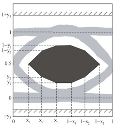
Figure 1. Transmission eye mask definition
| ||||||
Parameter | Symbol | Condition | Min. | Typical | Max. | Unit |
Channel data rate |
|
|
| 25.7812 |
| Gbps |
Data rate variation |
|
| -100 |
| +100 | ppm |
Lane Center Wavelength | λcT0 |
| 1294.53 | 1295.56 | 1296.59 | nm |
λcT1 |
| 1299.02 | 1300.05 | 1301.09 | nm | |
λcT2 |
| 1303.54 | 1304.58 | 1305.63 | nm | |
λcT3 |
| 1308.09 | 1309.14 | 1310.19 | nm | |
Damage threshold | PDT |
| - | 5.5 | - | dBm |
Average receiver power per | Rpow |
| -10.6 | - | 4.5 | dBm |
lane |
|
|
|
|
|
|
Receive power OMA per Lane | Rovl |
| - | - | 4.5 | dBm |
Difference in receive power between any two lanes(OMA) |
|
| - | - | 5.5 | dB |
Receiver Sensitivity(OMA) per lane | Psen |
| - | - | -8.6 | dBm |
Stressed Receiver Sensitivity per Lane | Psen_str |
|
|
| -6.8 | dBm |
Receiver Reflectance | Ref |
| - | - | -26 | dB |
Conditions of stressed receiver sensitivity test | ||||||
Vertical eye closure penalty per Lane |
|
| - | - | 1.8 | dB |
Stressed eye jitter per Lane |
|
| - | - | 0.3 | UI |
Rx-Lane LOS Assert |
|
| - | - | -12 | dBm |
Rx-Lane LOS Deassert |
|
| -13.6 | - | - | dBm |
Rx-Lane LOS Hysteresis |
|
| 0.5 | - | - | dB |
Transmitter Operating Characteristic-Optical (OTU4) |
|
| ||||
Parameter | Symbol | Condition | Min. | Typical | Max. | Unit |
Channel data rate |
|
|
| 27.9525 |
| Gbps |
Aggregate data rate |
|
|
| 111.809 |
| Gbps |
Data rate variation |
|
| -20 |
| +20 | ppm |
Lane Center Wavelength | λcT0 |
| 1294.53 | 1295.56 | 1296.59 | nm |
λcT1 |
| 1299.02 | 1300.05 | 1301.09 | nm | |
λcT2 |
| 1303.54 | 1304.58 | 1305.63 | nm | |
λcT3 |
| 1308.09 | 1309.14 | 1310.19 | nm | |
Total Average Launch Power | Pout |
| - | - | 8.9 | dBm |
Average Launch Power per Lane | Peach |
| -2.5 | - | 2.9 | dBm |
Optical Modulation Amplitude per Lane | OMA |
| -1.2 | - | 4.5 | dBm |
Difference in Launch power between any two lances(OMA) |
|
| - | - | 5.0 | dB |
Average Launch Power of TX_DIS Transmitter per lane | Poff | TX_DIS=H | - | - | -30 | dBm |
Extinction Ratio | ER |
| 7 | - | - | dB |
SMSR | SMSR |
| 30 | - | - | dB |
Relative Intensity Noise | RIN | Mod off | - | - | -130 | dB/Hz |
Opitcal Return Loss Tolerance | TRL |
| - | - | 20 | dB |
Transmitter reflectance | Tef |
| - | - | -26 | dB |
Optical Eye Mask {X1, X2, X3, Y1, Y2, Y3}1 | EMM |
| NRZ 25G RATIO {x1:0.25,x2:0.4,x3:0.45, y1:0.25,y2:0.28,y3:0.4} |
|
| |
Receiver Operating Characteristic-Optical (OTU4) |
|
| ||||
Parameter | Symbol | Condition | Min. | Typical | Max. | Unit |
Channel data rate |
|
|
| 27.9525 |
| Gbps |
Data rate variation |
|
| -20 |
| +20 | ppm |
Lane Center Wavelength | λcT0 |
| 1294.53 | 1295.56 | 1296.59 | nm |
λcT1 |
| 1299.02 | 1300.05 | 1301.09 | nm | |
λcT2 |
| 1303.54 | 1304.58 | 1305.63 | nm | |
λcT3 |
| 1308.09 | 1309.14 | 1310.19 | nm | |
Damage threshold | PDT |
| - | 5.5 | - | dBm |
Average receiver power per lane | Rpow |
| -8.8 | - | 2.9 | dBm |
Average total input power |
|
|
|
| 8.9 | dBm |
Channel power difference |
|
|
|
| 5.5 | dB |
Optical path penalty |
|
|
|
| 1.5 | dB |
Receiver Sensitivity per lane2 | Psen |
| - | - | -10.3 | dBm |
Receiver Reflectance | Ref |
| - | - | -26 | dB |
Rx-Lane LOS Assert |
|
| -13.6 | - | - | dBm |
Rx-Lane LOS Deassert |
|
| - | - | -12 | dBm |
Rx-Lane LOS Hysteresis |
|
| 0.5 | - | - | dB |
Sinusoidal Jitter, High Frequency |
|
|
|
| 0.05 | UIpp |
Notes:
[1] Please refer to Figure 1
[2] OTU-4 Rate without FEC, BER < 10-12, ER > 7dB
Electrical High Speed I/O Interface Characteristic-Transmitter(CEI-28G-VSR input interface) | ||||||
Parameter | Symbol | Condition | Min. | Typical | Max. | Unit |
Signal Rate Per Lane |
| 100GE |
| 25.7812 |
| Gb/s |
Signal Rate Per Lane |
| OTU4 |
| 27.9525 |
| Gb/s |
Signal Rate Tolerance |
| 100GE | -100 |
| 100 | ppm |
Signal Rate Tolerance |
| OTU4 | -20 |
| 20 | ppm |
Input Differential Voltage | Vdiff | Emphasis off | Note1 |
| 1200 | mV |
Differential Input Resistance | Rdin |
| 85 | 100 | 115 | Ω |
Input Impedance Mismatch | Rm |
|
|
| 5 | % |
Sinusoidal Jitter, Maximum |
|
|
|
| 5 | UIpp |
Notes:
[1] Meets CEI-28G-VSR compliance requirements
Electrical High Speed I/O Interface Characteristic-Receiver(CEI-28G-VSR output interface) | ||||||
Parameter | Symbol | Condition | Min. | Typical | Max. | Unit |
Signal Rate Per Lane |
| 100GE |
| 25.7812 |
| Gb/s |
Signal Rate Per Lane |
| OTU4 |
| 27.9525 |
| Gb/s |
Signal Rate Tolerance |
| 100GE | -100 |
| 100 | ppm |
Signal Rate Tolerance |
| OTU4 | -20 |
| 20 | ppm |
Output Differential Voltage | Vdiff | Equalization off | 600 | 750 | 900 | mV |
Differential Resistance | Rdo |
| 85 | 100 | 115 | Ω |
Differential Termination Resistance Mismatch | Rdm |
|
|
| 5 | % |
Output Rise and Fall Time | T_tr, T_tf | 20% to 80% |
|
| 15 | ps |
Common Mode Noise(RMS) | Ncm |
|
|
| 12 | mV |
Uncorrelated Unbounded Gaussian Jitter |
|
|
| 0.1 | 0.15 | UI |
Uncorrelated Bounded High Probability Jitter |
|
|
| 0.18 | 0.28 | UI |
Total Jitter | Tj |
|
| 0.28 | 0.43 | UI |
3.3V LVCMOS Electrical Low Speed I/O Interface Characteristic |
| |||||
Parameter | Symbol | Condition | Min. | Typical | Max. | Unit |
Supply Voltage | Vcc |
| 3.2 | 3.3 | 3.4 | V |
Input High Voltage | VIH |
| 2 |
| Vcc+0.3 | V |
Input Low Voltage | VIL |
| -0.3 |
| 0.8 | V |
Input Leakage Current | IIN |
| -10 |
| +10 | mA |
Output High Voltage (IOH =-100uA) | VOH |
| Vcc-0.2 |
| Vcc+0.3 | V |
Output Low Voltage (IOL =100uA) | VOL |
| -0.3 |
| 0.2 | V |
Minimum Pulse Width of Control Pin Signal | t_CNTL |
| 100 |
|
| us |
Notes.
(MOD_RSTn, MOD_LOPWR, TX_DIS, PRG_CNTL, MOD_ABS, RX_LOS, GLB_ALRMn, PRG_ALRM ) are
LVCMOS I/O interfaces.
Notes.
(MDIO, MDC, PRTADR4:0) are 1.2V LVCMOS I/O interfaces
Timing Parameters for CFP2 Hardware Signal Pins | ||||||
Parameter | Symbol | Condition | Min. | Typical | Max. | Unit |
Hardware MOD_LOPWR assert | t_MOD_LOPWR_assert |
|
|
| 1 | ms |
Hardware MOD_LOPWR deassert | t_MOD_LOPWR_deass ert |
|
|
| 10 | s |
Receiver Loss of Signal Assert Time | t_loss_assert |
|
|
| 100 | us1 |
Receiver Loss of Signal De-Assert Time | t_loss_deassert |
|
|
| 100 | us1 |
Global Alarm Assert Delay Time | GLB_ALRMn_assert |
|
|
| 150 | ms |
Global Alarm De-Assert Delay Time | GLB_ALRMn_deassert |
|
|
| 150 | ms |
Management Interface Clock Period | t_prd |
| 250 |
|
| ns |
Host MDIO t_setup | t_setup |
| 10 |
|
| ns |
Host MDIO t_hold | t_hold |
| 10 |
|
| ns |
CFP MDIO t_delay | t_delay |
| 0 |
| 175 | ns |
Initialization time from Reset | t_initialize |
|
|
| 2.5 | s |
Transmitter Disabled (TX_DIS asserted) | t_deassert |
|
|
| 100 | us |
Transmitter Enabled (TX_DIS de-asserted) | t_assert |
|
|
| 2 | ms |
Notes.
[1] Maximum value designed to support telecom applications
MDIO and MDC Timing Characteristics |
|
| ||||
Parameter | Symbol | Condition | Min. | Typical | Max. | Unit |
Management Interface Clock Frequency | F_MDC |
| 0.1 |
| 4 | MHz |
Management Interface Clock Period | t_prd |
| 250 |
| 10000 | ns |
Host MDIO t_setup | t_setup |
| 10 |
|
| ns |
Host MDIO t_hold | t_hold |
| 10 |
|
| ns |
CFP MDIO t_delay1 | t_delay |
| 0 |
| 175 | ns |
MDC high and low time | twidth |
| 40 |
| 60 | % |
| 160 |
|
| ns | ||
MDIO/MDC termination in CFP | Zt |
| 100 |
|
| kOhm |
Notes.
[1] Delay from MDC rising edge to MDIO data change.
Figure 2. MDIO & MDC Timing Diagram
Reference Clock Characteristics |
| |||||
Parameter | Symbol | Condition | Min. | Typical | Max. | Unit |
Impedance | Zd |
| 80 | 100 | 120 | ohm |
Frequency |
|
| 1/40 of host lane rate |
| ||
Frequency Stability | Xf |
| -100 |
| +100 | ppm1 |
| -20 |
| +20 | ppm2 | ||
Input Differential Voltage | Vdiff |
| 400 |
| 1200 | mV3 |
RMS Jitter | σ |
|
|
| 10 | ps4 |
Clock Duty Cycle |
|
| 40 |
| 60 | % |
Clock Rise/Fall Time 10/90% | Tr/f |
| 200 |
| 1250 | ps5 |
Notes.
[1] For Ethernet applications
[2] For Telecom applications
[3] Peak to Peak Differential
[4] Random Jitter. Over frequency band of 10kHz < f < 10MHz
[5] 1/40 of electrical lane
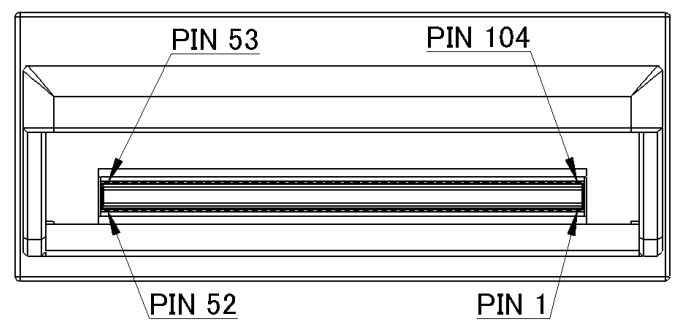
Figure 3. CFP2 Connector Pin Map Orientation
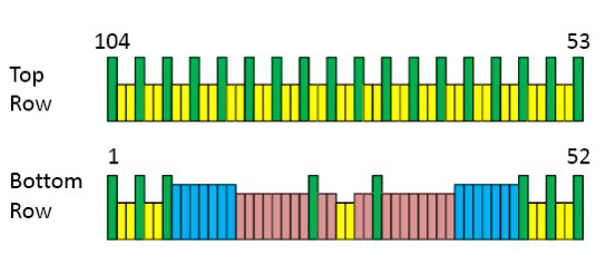
Figure 4. CFP2 Pin Map Connector
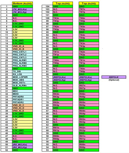
Figure 5. CFP2 Module Pin Map
Notes.
[1] Pin 15,16,36,37,38, are internally used and NOT allowed to connect any signal and power supply or GND.
[2] Pin 2,3,50,51 are disabled unless MCLK output is enabled via MDIO.
PIN | Name | I/O |
| Logic | Description |
1 | GND |
|
|
|
|
2 | (TX_MCLKn) | O | CML |
| Not Support |
3 | (TX_MCLKp) | O | CML |
| Not Support |
4 | GND |
|
|
|
|
5 | N.C |
|
|
| No Connect |
6 | N.C |
|
|
| No Connect |
7 | 3.3V_GND |
|
|
| 3.3V Module Supply Voltage Return Ground, can be |
8 | 3.3V_GND |
|
|
| separate or tied together with Signal Ground
|
9 | 3.3V |
|
|
| 3.3V Module Supply Voltage
|
3.3V |
|
| 3.3V Module Supply Voltage | ||
11 | 3.3V |
|
| 3.3V Module Supply Voltage | |
12 | 3.3V |
|
| 3.3V Module Supply Voltage | |
13 | 3.3V_GND |
|
|
| |
14 | 3.3V_GND |
|
|
| |
15 | VND_IO_A | I/O |
| Module Vendor I/O. Must No Connect at host board | |
16 | VND_IO_B | I/O |
| Module Vendor I/O. Must No Connect at host board | |
17 | PRG_CNTL1 |
I | LVCMOS w/ PUR | Programmable Control 1 set over MDIO, MSA Default: TRXIC_RSTn, TX & RX ICs reset, "0": reset, "1" or NC: enabled = not used 4.75kohm pull up in the module | |
18 | PRG_CNTL2 |
I | LVCMOS w/ PUR | Programmable Control 2 set over MDIO, MSA Default: Hardware Interlock LSB, "00": ≤3W, "01":≤6W, "10": ≤9W, "11" or NC: ≤12W = not used 4.75kohm pull up in the module | |
19 | PRG_CNTL3 |
I | LVCMOS w/ PUR | Programmable Control 3 set over MDIO, MSA Default: Hardware Interlock MSB, "00": ≤3W, "01": ≤6W, "10": ≤9W, "11" or NC: ≤12W = not used 4.75kohm pull up in the module | |
20 | PRG_ALRM1 |
O | LVCMOS | Programmable Alarm 1 set over MDIO, MSA Default: HIPWR_ON, "1": module power up completed, "0": module not high powered up | |
21 | PRG_ALRM2 |
O | LVCMOS | Programmable Alarm 2 set over MDIO, MSA Default: MOD_READY, "1": Ready, "0": not Ready. | |
22 | PRG_ALRM3 |
O | LVCMOS | Programmable Alarm 3 set over MDIO, MSA Default: MOD_FAULT, fault detected, "1": Fault, "0": No Fault | |
23 | GND |
|
|
| |
24 | TX_DIS |
I | LVCMOS w/ PUR | Transmitter Disable for all lanes, "1" or NC = transmitter disabled, "0" = transmitter enabled | |
25 | RX_LOS |
O | LVCMOS | Receiver Loss of Optical Signal, "1": low optical signal, "0": normal condition | |
26 | MOD_LOPWR |
I | LVCMOS w/ PUR | Module Low Power Mode. "1" or NC: module in low power (safe) mode, "0": power-on enabled 4.75kohm pull up in the module | |
27 | MOD_ABS |
O | GND | Module Absent. "1" or NC: module absent, "0": module present, Pull Up Resistor on Host | |
28 | MOD_RSTn | I | LVCMOS w/ PDR | Module Reset. "0" resets the module, "1" or NC = module enabled, 4.75kohm pull down in the module | |
29 | GLB_ALRMn |
O | LVCMOS | Global Alarm. “0": alarm condition in any MDIO Alarm register, "1": no alarm condition, Open Drain, Pull Up Resistor on Host
| |
30 | GND |
|
|
| |
31 | MDC |
I | 1.2V CMOS | Management Data Clock (electrical specs as per 802.3ae and ba) | |
32 | MDIO |
I/O | 1.2V CMOS | Management Data I/O bi-directional data (electrical specs as per 802.3ae and ba) | |
33 | PRTADR0 |
I | 1.2V CMOS | MDIO Physical Port address bit 0 | |
34 | PRTADR1 |
I | 1.2V CMOS | MDIO Physical Port address bit 1 | |
35 | PRTADR2 |
I | 1.2V CMOS | MDIO Physical Port address bit 2 | |
36 | VND_IO_C | I/O |
| Module Vendor I/O C. Do Not Connect! | |
37 | VND_IO_D | I/O |
| Module Vendor I/O D. Do Not Connect! | |
38 | VND_IO_E | I/O |
| Module Vendor I/O E. Do Not Connect! | |
39 | 3.3V_GND |
|
|
| |
40 | 3.3V_GND |
|
|
| |
41 | 3.3V |
|
| 3.3V Module Supply Voltage | |
42 | 3.3V |
|
| ||
43 | 3.3V |
|
| ||
44 | 3.3V |
|
| ||
45 | 3.3V_GND |
|
|
| |
46 | 3.3V_GND |
|
|
| |
47 | N.C |
|
| No Connect | |
48 | N.C |
|
| No Connect | |
49 | GND |
|
|
| |
50 | (RX_MCLKn) | O | CML | Not Support | |
51 | (RX_MCLKp) | O | CML | Not Support | |
52 | GND |
|
|
| |
PIN | Name | I/O | Logic | Description | ||
53 | GND |
|
|
| ||
54 | N.C |
|
| No Connect | ||
55 | N.C |
|
| No Connect | ||
56 | GND |
|
|
| ||
57 | RX0p | O | HS I/O | Lane 0 Receiver Output (Positive) | ||
58 | RX0n | O | HS I/O | Lane 0 Receiver Output (Negative) | ||
59 | GND |
|
|
| ||
60 | RX1p | O | HS I/O | Lane 1 Receiver Output (Positive) | ||
61 | RX1n | O | HS I/O | Lane 1 Receiver Output (Negative) | ||
62 | GND |
|
|
| ||
63 | N.C |
|
| No Connect | ||
64 | N.C |
|
| No Connect | ||
65 | GND |
|
|
| ||
66 | N.C |
|
| No Connect | ||
67 | N.C |
|
| No Connect | ||
68 | GND |
|
|
| ||
69 | RX2p | O | HS I/O | Lane 2 Receiver Output (Positive) | ||
70 | RX2n | O | HS I/O | Lane 2 Receiver Output (Negative) | ||
71 | GND |
|
|
| ||
72 | RX3p | O | HS I/O | Lane 3 Receiver Output (Positive) | ||
73 | RX3n | O | HS I/O | Lane 3 Receiver Output (Negative) | ||
74 | GND |
|
|
| ||
75 | N.C |
|
| No Connect | ||
76 | N.C |
|
| No Connect | ||
77 | GND |
|
|
| ||
78 | REFCLKp | I |
| Reference Clock Input (Positive), optional | ||
79 | REFCLKn | I |
| Reference Clock Input (Negative) , optional | ||
80 | GND |
|
|
| ||
81 | N.C |
|
| No Connect | ||
82 | N.C |
|
| No Connect | ||
83 | GND |
|
|
| ||
84 | TX0p | I | HS I/O | Lane 0 Transmitter Input (Positive) | ||
85 | TX0n | I | HS I/O | Lane 0 Transmitter Input (Negative) | ||
86 | GND |
|
|
| ||
87 | TX1p | I | HS I/O | Lane 1 Transmitter Input (Positive) | ||
88 | TX1n | I | HS I/O | Lane 1 Transmitter Input (Negative) | ||
89 | GND |
|
|
| ||
90 | N.C |
|
| No Connect | ||
91 | N.C |
|
| No Connect | ||
92 | GND |
|
|
| ||
93 | N.C |
|
| No Connect | ||
94 | N.C |
|
| No Connect | ||
95 | GND |
|
|
| ||
96 | TX2p | I | HS I/O | Lane 2 Transmitter Input (Positive) | ||
97 | TX2n | I | HS I/O | Lane 2 Transmitter Input (Negative) | ||
98 | GND |
|
|
| ||
99 | TX3p | I | HS I/O | Lane 3 Transmitter Input (Positive) | ||
100 | TX3n I |
| HS I/O | 99 Lane 3 Transmitter Input (Negative)
| ||
101 | GND |
|
|
| ||
102 | N.C |
|
| No Connect | ||
103 | N.C |
|
| No Connect | ||
104 | GND |
|
|
| ||
Dimensions
100Gb/s CFP2 mechanical dimensions should be compliant with CFP2 MSA specification. Detailed dimensions are shown in Figure 6.
(unit: mm)
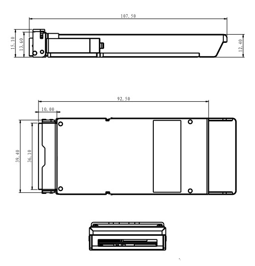
Figure 6. 100Gb/s CFP2 Mechanical Dimensions
The mechanical dimensions of the electrical connectors on the CFP2 Host PCB are shown in Figure 7.
(unit mm)
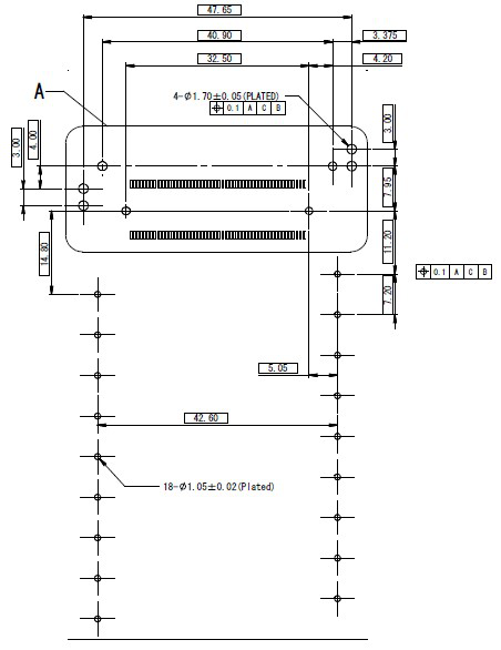
Figure 7 Mechanical Dimensions of Electrical Connectors on CFP2 Host PCB
| CFP2 Mechanical Characteristics | ||
| Max. | Unit | Notes |
Weight | 210 | g |
|
Flatness | 0.12 | mm |
|
Roughness | 1.6 | Ra |
|
CFP2 transceivers supports the MDIO interface specified in IEEE802.3 Clause 45. This 2-wire management data I/O interface is provided for the module status monitoring and control. The management data clock (MDC) provides clocking for the data that is passed on the MDIO port. Five further pins allow for loading of a port address (PORT_ADDR0-2) into the module.
Notes: Capacitor represents stray capacity 600ohm pull-up is preferred
For more detailed information please refer to " CFP MSA Management Interface Specification Version 2.2 r06".
Part No. |
|
| Specification |
|
| |
Pack | Rate | Tx | Rx | Reach | Connetor | |
MTRD-DG3CA | CFP2 | 103.1G 111.8G | 4*28G LAN-WDM EML TOSA | 4*28G PIN ROSA | 10km | LC |
Contact Information
Wuhan Huagong Genuine Optics Technology Co., Ltd
Address: Science & Technology Region of HUST, Donghu High-Tech Zone
Wuhan, Hubei Province, 430223, China
l Tel: +86-27-87180102
l Fax: +86-27-87180220


