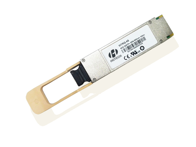

| 产品模块: | 40G Base-SR4 100m QSFP+ Optical Transceiver Module |
| 订购信息: | |
| 验证码: |
|
| 类 别: | 电子邮箱: | ||
| 电 话: | QQ: | ||
| *标题: | |||
| *留言内容: | |||
| *验证码: |
|
||
Description
MTRQ-4S100 transceiver is a Parallel 40Gb/s Quad Small Form-factor, Hot-Pluggable optical module.
The module integrates 4 independent transmitters and 4 independent receivers inside. Four-channel 850nm VCSEL array, PIN array,amplifier and Driver are used in the module for compact size, low power consumption and low cost. Each channel can operate at 10Gbps up to 100m using OM3 fiber, and 150m using OM4 fiber.
The transceiver is compliant to the industry standard SFF-8436 QSFP+ Transceiver Specification. Digital diagnostic functionsis provided to monitor the working state of the module. The electrical interface uses a 38 contact edge type connector. The optical interface uses an 8 or 12 fiber MTP (MPO) connector.
MTRQ-4S100 transceiver features small size, parallel multi- channel, hot-pluggable, low power and high speed operation. It’s very suitable for high speed short-distance density data connections such as 40G BASE-SR4, InfiniBand QDR, Switch& Route interconnects etc.
Features
l Compliant to the industry standard SFF-8436 QSFP+ Transceiver Specification
l 4* 10.3125Gbps per module, bi-directional operation
l 5 DDM with MPD monitor
l High reliability 850nm VCSEL array transmitter
l Hot pluggable
l Single 3.3V power supply, Low power consumption
l 0 to 70°C case temperature operating range
l RoHS-6 compliant (lead-free)
Applications
l 10GBASE-SR &40GBASE-SR4 40G Ethernet InfiniBand QDR (4 x 10G), DDR (4 x 5G) and SDR (4 x 2.5G) interconnects
l Datacom/Telecom Switch & Router connections
l High speed multi-channel parallel data connections
Compliance
l IEEE802.3ba 40GBASE-SR4
l SFF-8436 QSFP Specification
l InfiniBand Architecture QDR Specifications
Absolute Maximum Ratings | ||||||
Parameter | Symbols | Min | Typical | Max | Unit | Notes |
Storage Temperature | TSTG | -40 | - | +85 | ºC | |
Operating Temperature | Top | 0 | 70 | |||
Operating Relative Humidity | RH | 5 | - | 85 | % | |
3.3V Supply Voltage | VCC | -0.5 | - | +3.6 | V |
Recommended Operating Conditions | ||||||
Parameter | Symbols | Min | Typical | Max | Unit | Notes |
Case temperature | Tc | 0 | - | +70 | ℃ | |
3.3V Supply Voltage | VCC | 3.135 | 3.3 | 3.465 | V | |
Data Rate | 41.25 | Gbps | ||||
Receiver Differential Data Output Load | 100 | Ohms | ||||
Logic Input Voltage High | Vih | 2 | Vcc+0.3 | V | ||
Logic Input Voltage Low | Vil | -0.3 | 0.8 | V | ||
Two wire Serial Interface Clock Rate | 100 | 400 | KHz | |||
Power Supply Noise | 50 | mVpp | ||||
Fiber Length(OM3 2000MHz*Km) | 0.5 | 100 | m | |||
Fiber Length(OM44700MHz*Km) | 0.5 | 150 | m | |||
Electrical Characteristics | ||||||
Parameter | Symbles | Min | Type | Max | Unit | Notes |
Transceiver Power Consumption | 1.5 | W | ||||
Transceiver Power Supply Current | 475 | mA | ||||
Maximum peak Current | 900 | mA | ||||
Transceiver Power On Initialization Time | Tini | 2000 | ms | |||
Transmitter(per Lane) | ||||||
Differential Data Input Voltage Peak to Peak Swing | Vin,pp | 190 | 700 | mV | ||
Differential Input Impedance | Zind | 90 | 100 | 110 | ohm | AC Coupled Inside Module |
AC common-mode input voltage tolerance(RMS) | 15 | mV | ||||
Differential input return loss | Per IEEE P802.3ba, Section 86A.4.1.1 | dB | 10 MHz to 11.1 GHz | |||
J2 Jitter Tolerance | Jt2 | 0.3 | UI | |||
J9 Jitter Tolerance | Jt9 | 0.47 | UI | |||
Eye mask coordinates: (X1, X2, Y1, Y2) | 0.11, 0.31 95, 350 | UI mV | Hit ratio = 5 × 10⁻⁵ | |||
Transmitter eye mask definition {X1, X2, X3, Y1, Y2, Y3} | 0.23,0.34,0.43 0.27,0.35,0.4 | UI | Hit ratio = 5 × 10⁻⁵ | |||
Receiver(per Lane) | ||||||
Differential Data Output Voltage Peak to Peak Swing | Vopp | 300 | 850 | mV | ||
Differential output Impedance | Zos | 90 | 100 | 110 | 0hms | AC Coupled Inside Module |
Differential output return loss | Per IEEE P802.3ba, Section 86A.4.2.1 | dB | 10 MHz to 11.1 GHz | |||
J2 Output | Jo2 | 0.42 | UI | |||
J9 Output | Jo9 | 0.65 | UI | |||
Eye mask coordinates: (X1, X2, Y1, Y2) | 0.29, 0.5 150, 425 | UI mV | 10,Hit ratio = 1 × 10-12 | |||
Data output rise/fall time (20%~80%) | 28 | ps | 20% to 80% |
Optical Characteristics | ||||||
Parameter | Symbles | Min | Type | Max | Unit | Notes |
Transmitter(per Lane) | ||||||
Center wavelength | λ c | 840 | 850 | 860 | nm | |
RMS spectral width | SW | 0.65 | nm | |||
Average power, each lane(EOL) | TXP | -7.6 | 1 | dBm | ||
Difference in Power between any two lanes [OMA] | 6.5 | dB | ||||
Transmit OMA per Lane (EOL) | -5.6 | 3 | dBm | |||
Extinction Ratio | 3 | dB | ||||
TDP per Lane | TDP | 3.5 | dB | |||
Launch Power in OMA minus TDP, each lane | -6.5 | dBm | ||||
Optical Return Loss Tolerance | 12 | dB | ||||
Average launch power of OFF transmitter, per lane | -30 | dBm | ||||
Relative Intensity Noise | -128 | dB/Hz | ||||
Transmitter eye mask definition {X1, X2, X3, Y1, Y2, Y3} | 10% | IEEE802. 3ba | Hit ratio = 1 × 10-12 | |||
Receiver(per Lane) | ||||||
Center wavelength | λ c | 840 | 850 | 860 | nm | |
Saturation power(EOL) | 2.4 | dBm | ||||
Max Input power | 2.4 | dBm | ||||
Average power at receiver input, each lane | -9.5 | 2.4 | dBm | |||
Receive Power (OMA) per Lane | 3 | dBm | ||||
Peak Power, per lane | 4 | dBm | ||||
Sensitivity (OMA EOL),each lane | -11.1 | dBm | ||||
Stressed Receiver Sensitivity (OMA EOL) per Lane | -6.4 | dBm | ||||
Receiver Reflectance | -12 | dBm | ||||
Receiver jitter tolerance [OMA], each Lane | -5.4 | dBm | ||||
Rx_Loss assert | LOSA | -30 | dBm | |||
Rx_LossDe_assert | LOSD | -12 | dBm | |||
LOS Hysteresis | 0.5 | dB | ||||
Rx output squelch function | Yes | - | ||||
Rx LOS in signal or RSSI | RSSI | - | ||||
Laser status in reset | Close | - |
Digital Diagnostic Function | ||||||
Parameter | Symbles | Min | Type | Max | Unit | Notes |
Temperature DDMaccuracy | DMI_Temp | -3 | +3 | ℃ | ||
Supply voltage DDMaccuracy | DMI_VCC | -5% | +5% | V | ||
Rx power DDMaccuracy | DMI_Rx | -3 | +3 | dB | ||
Bias current DDM accuracy | DMI_Ibias | -10% | +10% | mA | ||
Tx power DDM accuracy | DMI_Tx | -3 | +3 | dB |

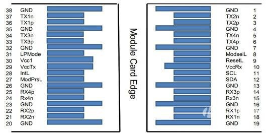
Top Side Bottom Side
Viewed from Top Viewed from Bottom
Figure 1 – QSFP+ MSA-compliant 38-pin connector
Pin Description
Pin | Name | Description | Notes | ||||||
1 | GND | Ground | Note1 | ||||||
2 | Tx2n | Transmitter Inverted Data Input | |||||||
3 | Tx2p | Transmitter Non-Inverted Data Input | |||||||
4 | GND | Ground | Note1 | ||||||
5 | Tx4n | Transmitter Inverted Data Input | |||||||
6 | Tx4p | Transmitter Non-Inverted Data Input | |||||||
7 | GND | Ground | |||||||
8 | ModSelL | Module Select | |||||||
9 | ResetL | Module Reset | |||||||
10 | Vcc Rx | +3.3V Power Supply Receiver | Note2 | ||||||
11 | SCL | 2-wire serial interface clock | |||||||
12 | SDA | 2-wire serial interface data | |||||||
13 | GND | Ground | |||||||
14 | Rx3p | Receiver Non-Inverted Data Output | |||||||
15 | Rx3n | Receiver Inverted Data Output | |||||||
16 | GND | Ground | Note1 | ||||||
17 | Rx1p | Receiver Non-Inverted Data Output | |||||||
18 | Rx1n | Receiver Inverted Data Output | Note1 | ||||||
19 | GND | Ground | Note1 | ||||||
20 | GND | Ground | |||||||
21 | Rx2n | Receiver Inverted Data Output | |||||||
22 | Rx2p | Receiver Non-Inverted Data Output | |||||||
23 | GND | Ground | |||||||
24 | Rx4n | Receiver Inverted Data Output | |||||||
25 | Rx4p | Receiver Non-Inverted Data Output | |||||||
26 | GND | Ground | Note1 | ||||||
27 | ModPrsL | Module Present | |||||||
28 | IntL | Interrupt | |||||||
29 | VccTx | +3.3V Power supply transmitter | Note2 | ||||||
30 | Vcc1 | +3.3V Power supply | Note2 | ||||||
31 | LPMode | Low Power Mode | |||||||
32 | GND | Ground | Note1 | ||||||
33 | Tx3p | Transmitter Non-Inverted Data Input | |||||||
34 | Tx3n | Transmitter Inverted Data Input | |||||||
35 | GND | Ground | Note1 | ||||||
36 | Tx1p | Transmitter Non-Inverted Data Input | |||||||
37 | Tx1n | Transmitter Inverted Data Input | |||||||
38 | GND | Ground | Note1 | ||||||
Notes:
[1] GND is the symbol for signal and supply (power) common for the QSFP+ module. All are common within the QSFP+ module and all module voltages are referenced to this potential unless otherwise noted. Connect these directly to the host board signal-common ground plane.
[2] Vcc Rx, Vcc1 and Vcc Tx are the receiver and transmitter power supplies and shall be applied concurrently.Recommended host board power supply filtering is shown in Figure 7. Vcc Rx Vcc1 and VccTx may be internally connected within the QSFP+ Module in any combination. The connector pins are each rated for a maximum current of 500 mA.

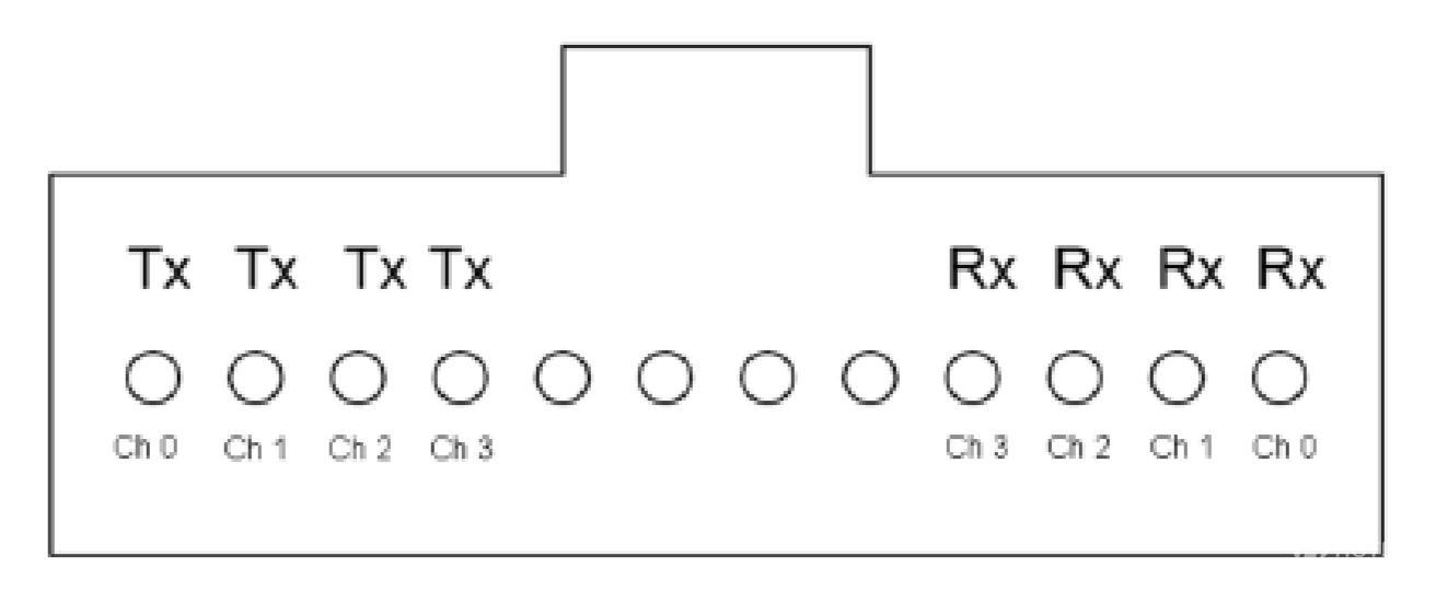
Figure 2 – Optical lane assignment (front view of MPO receptacle)
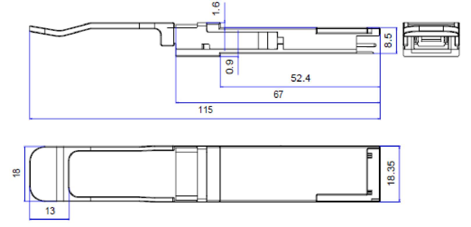
Unit is millimeter. All dimensions are ±0.1mm unless otherwise specified.

Figure3Mechanical Package Outline
Part No | Specification | ||||||||
Pack | Rate | Tx | Pout | Rx | S | Top | Reach | Others | |
MTRQ-4S100 | QSFP+ | 40G | 850nm VCSEL | -7.6~ 1dBm | PIN | <-11.1dBm | 0~70℃ | 100M(OM3) | DDM/RoHS |
Caution
All adjustments have been done at the factory before the shipment of the devices. No maintenance and user serviceable part is required. Tampering with and modifying the performance of the device will result in voided product warranty.
HG Genuine possesses the authority for ultimate explanation of all information contained in this document, which is subject to change without prior notice. All the information was obtained in specific environments; and HG Genuine will not be responsible for verifying the products performance in customers’ operating environments, neither liable for the performance of users' products. All information contained is only for the users' reference and shall not be considered as warranted characteristics. HG Genuine will not be liable for damages arising directly or indirectly from any use of the information contained in this document.
Publishing Date: 2015-09-10
Copyright Ó HG Genuine
All Right Reserved