华工正源中文站华工正源
- +86-27-87180102
-
社交媒体
 微信公众账号
 手机站
手机站
微信公众账号
手机站

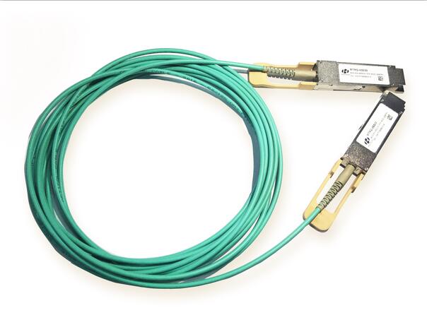
| 产品模块: | 40G QSFP+ SR4 Active Optical Cable |
| 订购信息: | |
| 验证码: |
|
| 类 别: | 电子邮箱: | ||
| 电 话: | QQ: | ||
| *标题: | |||
| *留言内容: | |||
| *验证码: |
|
||
Description
MTRQ-4S100 is a Four-Channel, Parallel,Fiber-Optic QSFP+ Avtive Optical Cable for 40G Base-SR4 Ethernet Applications. This transceiver is a high performance module for short-reach muti-lane data communication and interconnect applications.it integrates four data lanes in each direction with 41.25Gbps bandwidth. Each lane can operate during 4x1Gbps~4x10.3125Gbps.
These modules are designed to operate over multimode fiber systems using a nominal wavelength of 850nm. The electrical interface uses a 38 contact edge type connector. The optical interface uses an 12 fiber MTP(MPO) connector.
A serial EEPROM in the transceiver allows the user to access transceiver monitoring and configuration data via the 2-wire QSFP Management Interface. This interface uses a single address, A0h, with a memory map divided into a lower and upper area. Basic digital diagnostic (DD) data is held in the lower area while specific data is held in a series of tables in the high memory area.
Features
l Support Data Rate 4x1Gbps〜4x10.3125Gbps
l 4 channels 850nm VCSEL array
l 4 channels PIN photo detector array
l DDM function implemented
l Single MPO connector receptacle
l Hot Pluggable QSFP+ form factor
l Single +3.3V power supply
l Power consumption less than 1W
l Operating case temperature: 0〜+70°C
l Distance 1 m/3m/5m/10m/15m/20m/30m/50m/100m
Applications
l 1G/10G Ethernet
l Datacom/Telecom switch&router connections
l Data Aggregation and Backplane Applicationgs
l Infiniband transmission at 4ch QDR,FDR and EDR
Compliance
l Compliant with SFF-8436 Rev 2.7
l Compliant with IEEE 802.3ae
Specification
Absolute Maximum Ratings | ||||
Parameter | Symbol | Min. | Max. | Unit |
Storage Temperature | TS | -40 | +85 | ℃ |
Supply Voltage | VCC3 | 0 | 3.6 | V |
Relative Humidity | RH | 5 | 85 | % |
Recommended Operating Conditions | ||||||
Parameter | Symbol | Min. | Typical | Max. | Unit | Note |
Operating Case Temperature | TC | 0 | 70 | ℃ | ||
Power Supply Voltage | VCC3 | 3.13 | 3.3 | 3.47 | V | |
ICC3 | 300 | mA | ||||
Power Dissipation | PD | 1 | W | |||
Data Rate per channel | 1 | 10.3125 | Gbps | |||
Electrical Characteristic | ||||||
Parameter | Symbol | Min. | Typical | Max. | Unit | Note |
Input differential impedance | 100 | Ω | ||||
Differential data input swing | 180 | 700 | mV | |||
Differential data output swing | 300 | 850 | mV | |||
Transition Time, 20 to 80% | Tr, Tf | 28 | ps | |||
AC common-mode input voltage tolerance(RMS) | 15 | mV | ||||
Two Wire Serial (TWS) Interface Clock Rate | 400 | kHz |

Figure1
Pin | Name | Description | Notes |
1 | GND | Ground | Note1 |
2 | Tx2n | Transmitter Inverted Data Input | |
3 | Tx2p | Transmitter Non-Inverted Data Input | |
4 | GND | Ground | Note1 |
5 | Tx4n | Transmitter Inverted Data Input | |
6 | Tx4p | Transmitter Non-Inverted Data Input | |
7 | GND | Ground | |
8 | ModSelL | Module Select | |
9 | ResetL | Module Reset | |
10 | Vcc Rx | +3.3V Power Supply Receiver | Note2 |
11 | SCL | 2-wire serial interface clock | |
12 | SDA | 2-wire serial interface data | |
13 | GND | Ground | |
14 | Rx3p | Receiver Non-Inverted Data Output | |
15 | Rx3n | Receiver Inverted Data Output | |
16 | GND | Ground | Note1 |
17 | Rx1p | Receiver Non-Inverted Data Output | |
18 | Rx1n | Receiver Inverted Data Output | Note1 |
19 | GND | Ground | Note1 |
20 | GND | Ground | |
21 | Rx2n | Receiver Inverted Data Output | |
22 | Rx2p | Receiver Non-Inverted Data Output | |
23 | GND | Ground | |
24 | Rx4n | Receiver Inverted Data Output | |
25 | Rx4p | Receiver Non-Inverted Data Output | |
26 | GND | Ground | Note1 |
27 | ModPrsL | Module Present | |
28 | IntL | Interrupt | |
29 | VccTx | +3.3V Power supply transmitter | Note2 |
30 | Vcc1 | +3.3V Power supply | Note2 |
31 | LPMode | Low Power Mode | |
32 | GND | Ground | Note1 |
33 | Tx3p | Transmitter Non-Inverted Data Input | |
34 | Tx3n | Transmitter Inverted Data Input | |
35 | GND | Ground | Note1 |
36 | Tx1p | Transmitter Non-Inverted Data Input | |
37 | Tx1n | Transmitter Inverted Data Input | |
38 | GND | Ground | Note1 |
Notes:
[1] GND is the symbol for signal and supply (power) common for the QSFP+ module. All are common within the QSFP+ module and all module voltages are referenced to this potential unless otherwise noted. Connect these directly to the host board signal-common ground plane.
[2] Vcc Rx, Vcc1 and VccTx are the receiver and transmitter power supplies and shall be applied concurrently.Recommended host board power supply filtering is shown in Figure 7. Vcc Rx Vcc1 and VccTx may be internally connected within the QSFP+ Module in any combination. The connector pins are each rated for a maximum current of 500 mA.
Optical Interface Lanes and Assignment

Figure 2 Optical lane assignment (front view of MPO receptacle)
Mechanical Dimensions
Unit is millimeter. All dimensions are ±0.1mm unless otherwise specified.

Figure3 Mechanical Package Outline

Part No | Specification | |||||||
Pack | Rate | 4 Tx | Standard Cable Lengths | 4 Rx | Standard Optical Cable Type
| Case temperature | Others | |
MTRQ-4S100 AOC | QSFP+ | 4x1G~ 4x10.3125G | 850nm VCSEL | 1, 3, 5, 10, 15, 20, 30, 50, 100 | PIN | Multimode round fiber cable | 0~70℃ | DDM/RoHS |
Contact Information
Wuhan Huagong Genuine Optics Technology Co., Ltd
Address: Science & Technology Region of HUST, Donghu High-Tech Zone
Wuhan, Hubei Province, 430223, China
l Tel: +86-27-87180102
l Fax: +86-27-87180220
Email: market@genuine-opto.com
Website: http://www.genuine-opto.com
HG Genuine possesses the authority for ultimate explanation of all information contained in this document, which is subject to change without prior notice. All the information was obtained in specific environments; and HG Genuine will not be responsible for verifying the products performance in customers’ operating environments, neither liable for the performance of users' products. All information contained is only for the users' reference and shall not be considered as warranted characteristics. HG Genuine will not be liable for damages arising directly or indirectly from any use of the information contained in this document.
Publishing Date: 2016-10-20
Copyright Ó HG Genuine
All Right Reserved
