
| 产品模块: | XG PON N1 OLT XFP Transceiver |
| 订购信息: | |
| 验证码: |
|
| 类 别: | 电子邮箱: | ||
| 电 话: | QQ: | ||
| *标题: | |||
| *留言内容: | |||
| *验证码: |
|
||
Description
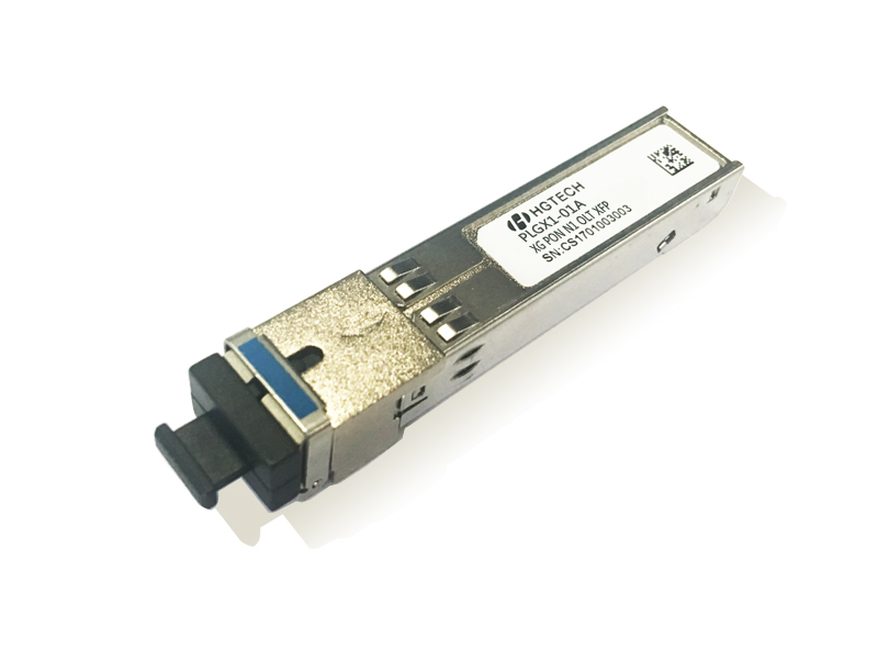
The HG Genuine PLGX1-01A transceiver consists 1577nm DFB EML laser, 1270nm APD photodiode WDM filter and Preamplifier in a high-integrated optical sub-assembly for 2.5G upstream and 10G downstream GPON applications up to 20km. The optical interface is SC/UPC receptacle. It adopts XFP Package. Power supply is single +3.3 Voltage.
Features
l XFP Package.
l Single Power Supply +3.3 Voltage.
l Single Fiber Bi-Directional SC/UPC receptacle.
l 1577nm continuous-mode 10.3125Gb/s DFB EML transmitter
l 1270nm burst-mode 2.5Gb/s APD receiver
l SFP electrical interface
l 2-wire interface for integrated Digital Diagnostic monitoring
l Operating temperature range: 0 °C ~+70 °C
Applications
l 10 Gigabit PON OLT application
Compliance
l Compliant with INF-8077i
l Compliant with IEEE 802.3av
l Compliant with IEC60825 Class 1
l RoHS compliance
Specification
Absolute Maximum Ratings | ||||||
Parameter | Symbol | Min | Typical | Max | Unit | Notes |
Storage Temperature | TSTG | -40 | 85 | ºC | ||
Operating Relative Humidity | 5 | 95 | % | |||
Supply Voltage | VCC | -0.5 | 4 | V | ||
Ambient temperature | Ta | -25 | - | +75 | ℃ | |
Recommended Operating Conditions | ||||||
Parameter | Symbol | Min | Typical | Max | Unit | Notes |
Case Operation Temperature | Ta | 0 | 70 | ºC | ||
Supply Voltage | VCC | 3.135 | 3.3 | 3.465 | V | |
Module Power Dissipation | P | 2.5 | W | |||
Tested under recommended operating conditions, unless otherwise noted
Transmitter OperatingCharacteristic-Optical,Electrical | ||||||
Parameter | Symbol | Min | Typical | Max | Units | Notes |
Data Rate | BR | 9.953 | Gb/s | |||
Differential Input Voltage | Vin p-p | 120 | - | 820 | mV | |
Output Optical Power | PO | 2.5 | - | 6 | dBm | BOL |
2 | - | 6 | dBm | EOL | ||
Extinction Ratio | ER | 8.2 | - | dB | ||
Center Wavelength Range | λc | 1575 | 1577 | 1580 | nm | |
Spectrum Width(-20dB) | Δλ | - | - | 1 | nm | DFB EML |
Side Mode Suppression Ratio | SMSR | 30 | - | - | dB | |
Transmitter Dispersion Penalty | Tdp | - | - | 1 | dB | |
Total jitter | TJ | - | - | 0.3 | UI | |
Output Optical Eye | Complies with IEEE802.3av eye masks when filtered | |||||
Tx_Disable Voltage | VOH | 2.0 | - | Vcc | V | LVTTL |
VOL | 0 | - | 0.8 | V | LVTTL | |
Laser turn on Time | Ton | 2 | ms | |||
Laser turn off Time | Toff | 10 | us | |||
Receiver Operating Characteristic-Optical,Electrical | ||||||
Parameter | Symbol | Min | Typical | Max | Units | Notes |
Differential Output Voltage | Vout p-p | 340 | 850 | mV | 50Ω load to Vcc-2V | |
Receiver Optical Wavelength | λIN | 1260 | 1270 | 1280 | nm | |
Receiver Sensitivity | Sen | -30.5 | dBm | BOL,Note1 | ||
-29.5 | dBm | EOL,Note1 | ||||
Overload Input Power | So | -7 | dBm | |||
SD of Signal Voltage | Nomal | 2.4 | Vcc | V | LVTTL | |
Fault | 0 | 0.4 | V | LVTTL | ||
SD Asserted | SD_A | -28.5 | dBm | |||
SD De-asserted | SD_D | -39 | dBm | |||
SD Hysteresis | PD- PA | 0.5 | 5 | dB | ||
Optical Return Loss | - | -20 | dB | |||
SD_A Settling Time | 50 | ns | ||||
SD_D Settling Time | 12.8 | ns | ||||
Reciever Dynamic range | 15 | dB | ||||
Reset Effective Level | HL | High | ||||
Reset Width | 64 | Bit | ||||
Data receiver Time | 64 | Bit | ||||
Notes:
[1]Measured with PRBS 2^23-1 test pattern @2.5Gbps with Tx on, ER=8.2dB, BER=10^-4.
Reliability Test Definitions and Distributions | |||||
Group | Test | Reference | Condition | SS[1] | C[2] |
Mechanical Integrity | Mechanical shock | MIL-STD-883 Method 2002.3 | 5 times/axis, 1500G, 0.5ms | 11 | 0 |
Vibration | MIL-STD-883 Method 2007.2 | 20G, 20~2000Hz, 4min/cys,4cys/axis | 11 | 0 | |
Thermal Shock | MIL-STD-883 Method 1011 | △T=100c 00C-1000C | 11 | 0 | |
Endurance | Accelerated Aging | GR-468-CORE | 85℃, 2000 hrs | 11 | - |
High temperature Storage | GR-468-CORE | 85℃, 2000 hrs | 11 | 0 | |
Low temperature Storage | GR-468-CORE | -40℃, 72 hrs | 11 | 0 | |
Temperature Cycles | MIL-STD-883 Method 1010.7 GR-468-CORE | -40℃~85℃ 500 cycles | 11 | 0 | |
Damp Heat | MIL-STD-202 Method 103 GR-468-CORE | 85 ℃,85%RH 1000 hrs | 11 | 0 | |
Cyclic moisture resistance | MIL-STD-883 Method 1004.7 GR-468-CORE | 20 cycles | 11 | 0 | |
Special Test | ESD threshold | MIL-STD-883E Method 3015.7 | 2000V HBM | 6 | 0 |
Note:
[1] SS: Sample Size;
[2] C: Maximum number of failure allowed in the test.
Digital Diagnostic Monitoring Information
Parameter | Range | Actual Value | Calibration Option | Note |
Transceiver Temperature | -40~85℃ | ±3℃ | Internal calibration | Recommended Operating Conditions |
Power Supply Voltage | 3.0-3.6V | ±3% | Internal calibration | Recommended Operating Conditions |
Tx Bias Current | 0~262mA | ±10% | Internal calibration | Recommended Operating Conditions |
Tx BM Optical Power | 2~6dBm | ±3dB | Internal calibration | Recommended Operating Conditions |
Rx Optical Power | -30.5~-7dBm | ±3dB | Internal calibration | Recommended Operating Conditions |
Pin-out Description

Pin Assignment
Pin | Name | Description |
1 | GND | Module Ground |
2 | Not Implemented | |
3 | Not Implemented | |
4 | Not Implemented | |
5 | TX_DIS | transmit disable; when high, transmitter output is turned OFF, Internal pull up |
6 | VCC5 | 5V power supply |
7 | GND | Module Ground |
8 | VCC3 | 3.3V power supply |
9 | VCC3 | 3.3V power supply |
10 | SCL | 2-Wire Serial Interface Clock |
11 | SDA | 2-Wire Serial Interface Data Line |
12 | Mod _ABS | Indicates Module is not present; Host shall put-up this pin and grounded in the module. When "High" the XFP module is absent from host board |
13 | RX_RST | Burst Receiver Reset |
14 | RX_SD | Burst Packet Detect, Higher level indicates that burst packet is detected by the receiver |
15 | GND | Module Ground |
16 | GND | Module Ground |
17 | RD- | Receive Burst Mode Inverted Data Output; DC coupled inside the module |
18 | RD+ | Receive Burst Mode Non-Inverted Data Output; DC coupled inside the module |
Figure Dimensions

Digital Diagnostic Memory Map

EEPROM Information
A0H | ||||
Addr. | Field Size | Name of Field | Hex | Description |
(Bytes) | ||||
0 | 1 | Identifier | 0x06 | XFP |
1 | 1 | Signal Conditioner Control | 0x00 | Data Rate:9.52Gb/s Normal Asynchronous REFCLK mode |
2-3 | 2 | Temperature High Alarm | 80℃ | MSB at low address |
4-5 | 2 | Temperature Low Alarm | -10℃ | MSB at low address |
6-7 | 2 | Temperature High Warning | 75℃ | MSB at low address |
8-9 | 2 | Temperature Low Warning | -5℃ | MSB at low address |
10-11 | 2 | Vcc High Alarm | 3.6V | MSB at low address |
12-13 | 2 | Vcc Low Alarm | 3.0V | MSB at low address |
14-15 | 2 | Vcc High Warning | 3.5V | MSB at low address |
16-17 | 2 | Vcc Low Warning | 3.1V | MSB at low address |
18-19 | 2 | 10G Bias High Alarm | XX | MSB at low address |
20-21 | 2 | 10G Bias Low Alarm | XX | MSB at low address |
22-23 | 2 | 10G Bias High Warning | XX | MSB at low address |
24-25 | 2 | 10G Bias Low Warning | XX | MSB at low address |
26-27 | 2 | 10G TX Power High Alarm | +7dBm | MSB at low address |
28-29 | 2 | 10G TX Power Low Alarm | +1dBm | MSB at low address |
30-31 | 2 | 10G TX Power High Warning | +6dBm | MSB at low address |
32-33 | 2 | 10G TX Power Low Warning | +2dBm | MSB at low address |
34-35 | 2 | RX Power high Alarm | -6dBm | MSB at low address |
36-37 | 2 | RX Power Low Alarm | -28.5dBm | MSB at low address |
38-39 | 2 | RX Power high Warning | -7dBm | MSB at low address |
40-41 | 2 | RX Power Low Warning | -27.5dBm | MSB at low address |
42-43 | 2 | Reserved | ||
44-45 | 2 | Reserved | ||
46-47 | 2 | Reserved | ||
48-49 | 2 | Reserved | ||
50-51 | 2 | Reserved | ||
52-53 | 2 | Reserved | ||
54-55 | 2 | Reserved | ||
56-57 | 2 | Reserved | ||
58-59 | 2 | Variable power control | 0x00 | Reserved |
60-69 | 10 | XX | ||
70-71 | 2 | Actual BER | XX | Actual BER Reported by the FEC to the Module |
72-75 | 4 | Wavelength Set | XXXX | User input of Wavelength setpoint |
76-79 | 4 | FEC control | XXXX | FEC control register |
80-87 | 8 | Alarm and Warning Flag | XXXXXXXX | Latched Alarm and Warning Falg(See Alarm/Warning Falg table) |
88-95 | 8 | Masking Alarm and Warning Falg | XXXXXXXX | Alarm and Warning Falg Masking register(See Masking Alarm/Warning Falg table) |
96-109 | 14 | Diagnostic Value | XXXXXXXXXXXXXX | Display real-time monitoring A/D(See Diagnostic Monitor table) |
110-111 | 2 | Control/status | XX | See General Control/Status Bits Table |
112-117 | 6 | Reserved | ||
118 | 1 | error Checking | 0x00 | Disable Packet Error Checking |
119-122 | 4 | New Password Entry | XXXX | Location of Entry of New Optional Password |
123-126 | 4 | Password Entry | XXXX | Location for Entry of Optional Password |
127 | 1 | Table Select | X | Entry Location for Table Select Byte |
Alarm/Warning Falg table
Addr. | Bit | Name of Field | Description |
80 | 7 | Temp High Alarm Flag | Latched high Temperature alarm |
80 | 6 | Temp Low Alarm Flag | Latched Low Temperature alarm |
80 | 5 | Vcc3 High Alarm Flag | Latched high Vcc3 alarm |
80 | 4 | Vcc3 Low Alarm Flag | Latched Low Vcc3 alarm |
80 | 3 | 10G Bias High Alarm Flag | Latched high 10G Bias alarm |
80 | 2 | 10G Bias Low Alarm Flag | Latched Low 10G Bias alarm |
80 | 1 | 10G TX Power High Alarm Flag | Latched high 10G TX Power alarm |
80 | 0 | 10G TX Power Low Alarm Flag | Latched Low 10G TX Power alarm |
81 | 7 | RX Power High Alarm Flag | Latched high RX Power alarm |
81 | 6 | RX Power Low Alarm Flag | Latched Low RX Power alarm |
81 | 5 | Reserved | |
81 | 4 | Reserved | |
81 | 3 | Reserved | |
81 | 2 | Reserved | |
81 | 1 | Reserved | |
81 | 0 | Reserved | |
82 | 7 | Temp High Warning Flag | Latched high Temperature Warning |
82 | 6 | Temp Low Warning Flag | Latched Low Temperature Warning |
82 | 5 | Vcc3 High Warning Flag | Latched high Vcc3 Warning |
82 | 4 | Vcc3 Low Warning Flag | Latched Low Vcc3 Warning |
82 | 3 | 10G Bias High Warning Flag | Latched high 10G Bias Warning |
82 | 2 | 10G Bias Low Warning Flag | Latched Low 10G Bias Warning |
82 | 1 | 10G TX Power High Warning Flag | Latched high 10G TX Power Warning |
82 | 0 | 10G TX Power Low Warning Flag | Latched Low 10G TX Power Warning |
83 | 7 | RX Power High Warning Flag | Latched high RX Power Warning |
83 | 6 | RX Power Low Warning Flag | Latched Low RX Power Warning |
83 | 5 | Reserved | |
83 | 4 | Reserved | |
83 | 3 | Reserved | |
83 | 2 | Reserved | |
83 | 1 | Reserved | |
83 | 0 | Reserved | |
84 | 7 | 10G TX_NR Status | Latched 10G TX_NR Status |
84 | 6 | 10G TX_Fault Status | Latched 10G TX_Fault Status |
84 | 5 | 10G TX CDR not Locked | Latched TX CDR Loss of Lock |
84 | 4 | 10G RX_NR Status | Latched 10G RX_NR Status |
84 | 3 | RX_SD Status | Latched mirror of RX_SD pin (Receiver loss |
84 | 2 | 10G RX CDR not Locked | Latched RX CDR Loss of Lock |
84 | 1 | MOD_NR Status | Latched MOD_NR status |
84 | 0 | Reset Complete | Latched Reset Complete Flag |
85 | 7 | APD Supply Fault | Latched APD Supply Fault |
85 | 6 | TEC Fault | Latched TEC Fault |
85 | 5 | Wavelength Unlocked | Latched Wavelength Unlocked Condition |
85 | 4-0 | Reserved | |
86 | 7 | VCC5 High Alarm | Latched VCC5 High Alarm Flag |
86 | 6 | VCC5 Low Alarm | Latched VCC5 Low Alarm Flag |
86 | 5 | Vcc3 High Alarm Flag | Latched Vcc3 high alarm Flag |
86 | 4 | Vcc3 Low Alarm Flag | Latched Vcc3 Low alarm Flag |
86 | 3 | VCC2 High Alarm | Latched Vcc2 high alarm Flag |
86 | 2 | Vcc2 Low Alarm Flag | Latched Vcc2 Low alarm Flag |
86 | 1 | Vee5 High Alarm | Latched Vee5 High Alarm Flag |
86 | 0 | Vee5 Low Alarm | Latched Vee5 Low Alarm Flag |
87 | 7 | VCC5 High Warning | Latched VCC5 High Warning Flag |
87 | 6 | VCC5 Low Warning | Latched VCC5 Low Warning Flag |
87 | 5 | Vcc3 High Warning Flag | Latched Vcc3 high Warning Flag |
87 | 4 | Vcc3 Low Warning Flag | Latched Vcc3 Low Warning Flag |
87 | 3 | VCC2 High Warning | Latched Vcc2 high Warning Flag |
87 | 2 | Vcc2 Low Warning Flag | Latched Vcc2 Low Warning Flag |
87 | 1 | Vee5 High Warning | Latched Vee5 High Warning Flag |
87 | 0 | Vee5 Low Warning | Latched Vee5 Low Warning Flag |
Masking Alarm/Warning Falg table
Addr. | Bit | Name of Field | Description |
88 | 7 | Temp High Alarm Flag | Masking bit for high Temperature alarm |
88 | 6 | Temp Low Alarm Flag | Masking bit for Low Temperature alarm |
88 | 5 | Vcc3 High Alarm Flag | Masking bit for high Vcc3 alarm |
88 | 4 | Vcc3 Low Alarm Flag | Masking bit for Low Vcc3 alarm |
88 | 3 | 10G Bias High Alarm Flag | Masking bit for high 10G Bias alarm |
88 | 2 | 10G Bias Low Alarm Flag | Masking bit for Low 10G Bias alarm |
88 | 1 | 10G TX Power High Alarm Flag | Masking bit for high 10G TX Power alarm |
88 | 0 | 10G TX Power Low Alarm Flag | Masking bit for Low 10G TX Power alarm |
89 | 7 | RX Power High Alarm Flag | Masking bit for high RX Power alarm |
89 | 6 | RX Power Low Alarm Flag | Masking bit for Low RX Power alarm |
89 | 5 | Reserved | |
89 | 4 | Reserved | |
89 | 3 | Reserved | |
89 | 2 | Reserved | |
89 | 1 | Reserved | |
89 | 0 | Reserved | |
90 | 7 | Temp High Warning Flag | Masking bit for high Temperature Warning |
90 | 6 | Temp Low Warning Flag | Masking bit for Low Temperature Warning |
90 | 5 | Vcc3 High Warning Flag | Masking bit for high Vcc3 Warning |
90 | 4 | Vcc3 Low Warning Flag | Masking bit for Low Vcc3 Warning |
90 | 3 | 10G Bias High Warning Flag | Masking bit for high 10G Bias Warning |
90 | 2 | 10G Bias Low Warning Flag | Masking bit for Low 10G Bias Warning |
90 | 1 | 10G TX Power High Warning Flag | Masking bit for high 10G TX Power Warning |
90 | 0 | 10G TX Power Low Warning Flag | Masking bit for Low 10G TX Power Warning |
91 | 7 | RX Power High Warning Flag | Masking bit for high RX Power Warning |
91 | 6 | RX Power Low Warning Flag | Masking bit for Low RX Power Warning |
91 | 5 | Reserved | |
91 | 4 | Reserved | |
91 | 3 | Reserved | |
91 | 2 | Reserved | |
91 | 1 | Reserved | |
91 | 0 | Reserved | |
92 | 7 | 10G TX_NR Status | Masking bit for 10G TX_NR Status |
92 | 6 | 10G TX_Fault Status | Masking bit for 10G TX_Fault Status |
92 | 5 | 10G TX CDR not Locked | Masking bit for TX CDR Loss of Lock |
92 | 4 | 10G RX_NR Status | Masking bit for 10G RX_NR Status |
92 | 3 | RX_SD Status | Masking bit for mirror of RX_SD pin (Receiver loss |
92 | 2 | 10G RX CDR not Locked | Masking bit for RX CDR Loss of Lock |
92 | 1 | MOD_NR Status | Masking bit for MOD_NR status |
92 | 0 | Reset Complete | Masking bit for Reset Complete Flag |
93 | 7 | APD Supply Fault | Masking bit for APD Supply Fault |
93 | 6 | TEC Fault | Masking bit for TEC Fault |
93 | 5 | Wavelength Unlocked | Masking bit for Wavelength Unlocked Condition |
93 | 4-0 | Reserved | |
94 | 7 | VCC5 High Alarm | Masking bit for VCC5 High Alarm Flag |
94 | 6 | VCC5 Low Alarm | Masking bit for VCC5 Low Alarm Flag |
94 | 5 | Vcc3 High Alarm Flag | Masking bit for Vcc3 high alarm Flag |
94 | 4 | Vcc3 Low Alarm Flag | Masking bit for Vcc3 Low alarm Flag |
94 | 3 | VCC2 High Alarm | Masking bit for Vcc2 high alarm Flag |
94 | 2 | Vcc2 Low Alarm Flag | Masking bit for Vcc2 Low alarm Flag |
94 | 1 | Vee5 High Alarm | Masking bit for Vee5 High Alarm Flag |
94 | 0 | Vee5 Low Alarm | Masking bit for Vee5 Low Alarm Flag |
95 | 7 | VCC5 High Warning | Masking bit for VCC5 High Warning Flag |
95 | 6 | VCC5 Low Warning | Masking bit for VCC5 Low Warning Flag |
95 | 5 | Vcc3 High Warning Flag | Masking bit for Vcc3 high Warning Flag |
95 | 4 | Vcc3 Low Warning Flag | Masking bit for Vcc3 Low Warning Flag |
95 | 3 | VCC2 High Warning | Masking bit for Vcc2 high Warning Flag |
95 | 2 | Vcc2 Low Warning Flag | Masking bit for Vcc2 Low Warning Flag |
95 | 1 | Vee5 High Warning | Masking bit for Vee5 High Warning Flag |
95 | 0 | Vee5 Low Warning | Masking bit for Vee5 Low Warning Flag |
Diagnostic Monitor table
Addr. | Field Size | Name of Field | Description |
(Bytes) | |||
96-97 | 2 | Measured Temperature | Yield a 16-bit A/D value, MSB at low address |
98-99 | 2 | Measured Vcc3 | Yield a 16-bit A/D value, MSB at low address |
100-101 | 2 | Measured 10G TX Bias | Yield a 16-bit A/D value, MSB at low address |
102-103 | 2 | Measured 10G TX Power | Yield a 16-bit A/D value, MSB at low address |
104-105 | 2 | Measured RX Power | Yield a 16-bit A/D value, MSB at low address |
106-107 | 2 | Reserved | |
108-109 | 2 | Reserved |
External calibration constant setting and reservation functions
Table 00h | |||
Addr. | Field Size | Name of Field | Description |
(Bytes) | |||
128-131 | 4 | RX Power Calibration Data4 | Single precision floating-point numbers (various values at each device) |
132-135 | 4 | RX Power Calibration Data3 | |
136-139 | 4 | RX Power Calibration Data2 | |
140-143 | 4 | RX Power Calibration Data1 | |
144-147 | 4 | RX Power Calibration Data0 | |
148-255 | 108 | Reserved | |
General Control/Status Bits Table
Addr. | Bit | Name of Field | Description |
110 | 7 | 10G TX Disable State | Digital state of the 10G TX Disable Input Pin. Updated within 100msec of change on pin |
110 | 6 | Soft 10G TX Disable | Optional read/write bit that allows software disable of laser. Writing '1' disables laser. Turn on/off time is 100 msec max from acknowledgement of serial byte transmission. This bit is “OR”d with the hard TX_DISABLE pin value. Note, per SFP MSA TX_DISABLE pin is default enabled unless pulled low by hardware. If Soft 10G TX Disable is not implemented, the transceiver ignores the value of this bit. Default power up value is 0 |
110 | 5 | MOD_NR State | Digital state of the MOD_NR Pin. Updated within 100msec of change on pin |
110 | 4 | P_Down State | Digital state of the P_Down Pin. Updated within 100msec of change on pin |
110 | 3 | Soft P_Down | Optional read/write bit that allows the module to be placed in the power down mode. This is identical to the P_Down hardware pin function except that it does not initiate a system reset |
110 | 2 | Interrupt | Digital state of the Interrupt output pin |
110 | 1 | RX_LOS | Indicates Optical Loss of Signal (per relevant optical link standard). Updated within 100msec of change on pin |
110 | 0 | Data_Not_Ready | Indicates transceiver has achieved power up and A/D data is ready. Bit remains high until data is ready to be read at which time the device sets the bit low |
111 | 7 | TX_NR State | Identifies Not Ready condition as specific to the TX path |
111 | 6 | TX_Fault State | Identifies Laser fault condition (Generated by laser safety system) |
111 | 5 | TX_CDR not Locked | Identifies Loss of Lock in TX path CDR |
111 | 4 | RX_NR State | Identifies Not Ready condition as specific to the TX path |
111 | 3 | RX_CDR not Locked | Identifies Loss of Lock in RX path CDR |
111 | 2 | Reserved | |
111 | 1 | Reserved | |
111 | 0 | Reserved |
Serial ID: Data Fields
Table 01h | ||||
Addr. | Field Size | Name of Field | Hex | Description |
(Bytes) | ||||
128 | 1 | Identifier | 06 | Type of serial transceiver |
129 | 1 | Ext. Identifier | D0 | Extended identifier of type of serial transceiver |
130 | 1 | Connector | 01 | SC/UPC |
131-138 | 8 | Transceiver | XXXXXXXX | |
139 | 1 | Encoding | 10 | NRZ |
140 | 1 | BR-Min | 63 | 9.95Gbit/S |
141 | 1 | BR-MAX | 63 | 9.95Gbit/S |
142 | 1 | Length(9um,km) | 14 | 20km |
143 | 1 | Length (9um) 100m | 00 | Transceiver transmit distance |
144 | 1 | Length (50um)10m | 00 | Transceiver transmit distance |
145 | 1 | Length (62.5um) 10m | 00 | Transceiver transmit distance |
146 | 1 | Length (Copper) | 00 | Not compliant |
147 | 1 | Device Technology | F6 | Top 4Bits for Transmitter Technology “F” means “Reserved”; Low 4 Bits “6” means cooled transmitter and APD detector |
148-163 | 16 | Vendor name | 48 47 20 47 45 4E 55 49 4E 45 20 20 20 20 20 20 | “HG GENUINE” (ASCII) |
164 | 1 | CDR Support | 00 | Without CDR |
165-167 | 3 | Vendor OU | 00 00 00 | |
168-183 | 16 | Vendor PN | 50 4C 47 58 31 2D 30 31 41 20 20 20 20 20 20 20 | “PLGX1-01A” (ASCII) |
184-185 | 2 | Vendor rev | 00 00 | |
186-187 | 2 | Wavelength | 7B 34 | 1577nm |
188-189 | 2 | Wavelength Tolerance | 03 E8 | 5nm |
190 | 1 | Max Case Temp | 4B | 75℃ |
191 | 1 | CC_BASE | XX | Check code for Base ID Fields (addresses 128-190) |
192-195 | 4 | Power Supply | C8 00 8A 00 | 4W,5V(400mA),3.3V(1A) |
196-211 | 16 | Vendor SN | 4D 41 30 39 30 31 30 30 33 30 30 31 33 20 20 20 | Serial Number of transceiver(ASCII). For example “MA09010030013” |
212-219 | 8 | Date code | 31 35 30 37 32 30 20 20 | Manufactory date code. For example“150720” |
220 | 1 | Diagnostic Monitoring Type | 08 | No BER Support, Average Power |
221 | 1 | Enhanced Options | 40 | soft TX_Disable implemented |
222 | 1 | Aux Monitorin | 00 | |
223 | 1 | CC_EXT | XX | Check code for the Extended ID Fields (addresses 192 to 222) |
224-255 | Reserved | |||
Digital Diagnostic Monitoring Accuracy
Addr | Parameter | Range | Unit | Accuracy |
96-97 | Temperature | -40℃ to 85℃ | ℃ | ±3 |
98-99 | Supply Voltage(3.3V) | 3.0V to 3.6V | V | ±3% |
100-101 | Tx Bias Current | 0 mA to 262mA | mA | ±10% |
102-103 | Tx Optical Power | 2dBm to 6dBm | dB | ±3 |
104-105 | Rx Optical Power | -27.5dBm to -7dBm | dB | ±3 |
Reset Timing Characteristics

PARAMETER | SYMBOL | MIN | TYP | MAX | UNITS |
SD Assert Time | Tsda1 | 0 | - | 5 | ns |
SD Assert Time | Tsda2 | 0 | - | 5 | ns |
SD DeAssert Time | Tsdd | 0 | - | 12.8 | ns |
Reset Width | Trw | 25.6 | - | - | ns |
Data recovery time | Trec | - | - | 25.6 | ns |
Reset To ONU Optical Time | Trto | 0 | - | 250 | us |
Reset Guard Time | Trg | 0 | - | 250 | us |
Reset Delay Time during Ranging | Trdr | 0 | - | - | ns |
Reset Delay Time during Operating | Trdo | 0 | - | - | ns |
Timing Characteristics for Digital RSSI

PARAMETER | SYMBOL | MIN | TYP | MAX | UNITS |
Packet Length | - | 300 | - | - | ns |
Trigger delay | Td | 25 | - | - | ns |
RSSI Trigger and Sample Time | Tw | 500 | - | - | ns |
Internal delay | Ts | 500 | - | - | us |
Ordering Information
Part No. | Specification | ||||||||
Pack | Rate | Tx | Pout | Rx | S | Top | Reach | Others | |
PLGX1-01A | XFP | 2.5Gb/s U 10.3125Gb/s D | 1577nm DFB EML | +2-+6dBm | APD | <-30.5dBm @2.5G | 0-70℃ | 20km | DDM /ROHS |
Contact Information
Wuhan Huagong Genuine Optics Technology Co., Ltd
Address: Science & Technology Region of HUST, Donghu High-Tech Zone
Wuhan, Hubei Province, 430223, China
l Tel: +86-27-87180102
l Fax: +86-27-87180220
Email: market@genuine-opto.com
Website: http://www.genuine-opto.com
Statement
HG Genuine possesses the authority for ultimate explanation of all information contained in this document, which is subject to change without prior notice. All the information was obtained in specific environments; and HG Genuine will not be responsible for verifying the products performance in customers’ operating environments, neither liable for the performance of users' products. All information contained is only for the users' reference and shall not be considered as warranted characteristics. HG Genuine will not be liable for damages arising directly or indirectly from any use of the information contained in this document.
Publishing Date: 2016-1-7
Copyright Ó HG Genuine
All Right Reserved


