华工正源中文站华工正源
- +86-27-87180102
-
社交媒体
 微信公众账号
 手机站
手机站
微信公众账号
手机站

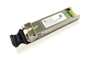
| 产品模块: | 25G 1310nm 10km SM SFP28 Transceiver |
| 订购信息: | |
| 验证码: |
|
| 类 别: | 电子邮箱: | ||
| 电 话: | QQ: | ||
| *标题: | |||
| *留言内容: | |||
| *验证码: |
|
||
Description
MTRA-3E30A is a high performance, cost effective modules, which is supporting Multi Rate 9.953-25.78Gbps, and transmission distance up to 10km on SM fiber. The transceiver consists of two sections: The transmitter section incorporates a 1310nm DFB Laser, a driver and a CDR. The receiver section consists of a PIN photodiode integrated with a transimpedance preamplifier (TIA), a Limitting Amplifier and CDR. The module is hot pluggable into the 20-pin connector. The high-speed electrical interface is base on low voltage logic, with nominal 100 Ohms differential impedance and AC coupled in the module.
The optical output can be disabled by LVTTL logic high-level input of TX_DIS. Transmit Fault (Tx_Fault) is provided to indicate that the module transmitter has detected a fault condition related to laser operation or safety. Loss of signal (RX_LOS) output is provided to indicate the loss of an input optical signal of receiver.
A serial EEPROM in the transceiver allows the user to access transceiver monitoring and configuration data via the 2-wire SFP
Management Interface. Digital diagnostics function are available via a 2-wire serial interface, as specified in SFF-8472.
Features
l Up to 10KM transmission distance
l Support Multi Rate 9.953-25.78Gbps
l 1310nm DFB and PIN receiver
l SFI electrical interface
l 2-wire interface for integrated Digital Diagnostic monitoring
l SFP+ MSA package with duplex LC connector
l H ot pluggable
l Very low EMI and excellent ESD protection
l +3.3V power supply
l Power consumption less than 1.5W
l Operating case temperature: 0~70°C
Applications
l 25Gbps Ethernet
l Compliant with IEEE 802.3-2012
l Compliant with FCC 47 CFR Part 15, Class B
l Compliant with MSA SFF-8472
l Compliant with MSA SFF-8431
|
Absolute Maximum Ratings |
|
|
|
|
|
Parameter |
Symbol |
Min. |
Max. |
Unit |
|
Storage Temperature |
TS |
-40 |
85 |
℃ |
|
Supply Voltage(no damaged) |
VCC3 |
-0.5 |
3.6 |
V |
|
Relative Humidity(non-condensing) |
RH |
5 |
95 |
% |
|
RX Input OMA Power |
Pmax |
|
5 |
dBm |
|
Recommended Operating Conditions |
|
|
|
|
|
|
Parameter |
Symbol |
Min. |
Typical |
Max. |
Unit |
|
Operating Case Temperature |
TC |
0 |
25 |
70 |
℃ |
|
Power Supply Voltage |
VCC3 |
3.135 |
3.3 |
3.465 |
V |
|
ICC3 |
|
|
400 |
mA |
|
|
Power Dissipation |
PD |
|
1.2 |
1.5 |
W |
|
Data Rate(NRZ) |
|
24.33 |
25.78 |
|
Gbps |
|
Transmission Distance |
|
|
|
10 |
Km |
|
Transmitter Operating Characteristic-Optical, Electrical |
|
|
||||
|
Parameter |
Symbol |
Min. |
Typical |
Max. |
Unit |
Note |
|
Centre Wavelength |
λC |
1290 |
1310 |
1325 |
nm |
|
|
Side Mode Suppression Ratio |
SMSR |
30 |
|
|
dB |
|
|
Laser Off Power |
Poff |
|
|
-30 |
dBm |
|
|
Average Optical Power |
Pavg |
-4.5 |
|
4.5 |
dBm |
|
|
Extinction Ratio |
ER |
4 |
|
|
dB |
|
|
Transmitter Dispersion Penalty |
|
|
|
2.7 |
dB |
|
|
Relative Intensity Noise |
Rin |
|
|
-130 |
dB/Hz |
|
|
Optical Return Loss Tolerance |
|
12 |
|
|
dB |
|
|
Operating Data Rate |
|
24.33 |
25.78 |
|
Gbps |
Note1 |
|
Optical Eye Mask |
>5% (Compatible 100GBASE-LR4) |
|
Note 2 |
|||
|
Common mode voltage tolerance |
|
15 |
|
|
mV |
|
|
Tx Input Diff Voltage |
VI |
200 |
500 |
900 |
mV |
|
|
Tx Fault |
VOL |
|
|
0.4 |
V |
At 0.7mA Note3 |
|
VOH |
VccT-0.4 |
|
|
|
||
Notes:
[1]Under CDR bypass mode, CPRI option 7 compatibility
[2] 1000 consecutive snapshots at typical rate and room temperature
[3] Measured with a 4.7k Ohm load pulled up to Vcc
|
Receiver Operating Characteristic-Optical, Electrical |
|
|
|
|
||
|
Parameter |
Symbol |
Min. |
Typ. |
Max. |
Unit |
Note |
|
Center Wavelength |
λr |
1260 |
1310 |
1360 |
nm |
|
|
Receiver Sensitivity(OMA) |
|
|
|
-14 |
dBm |
Note 1 |
|
LOS Assert |
LosA |
-30 |
|
|
dBm |
|
|
LOS Dessert |
LosD |
|
|
-13 |
dBm |
|
|
LOS Hysteresis |
LosH |
0.5 |
|
|
dB |
|
|
Overload(OMA) |
Pin |
4.5 |
|
|
dBm |
|
|
Receiver Reflectance |
|
|
|
-26 |
dB |
|
|
Operating Data Rate |
|
24.33 |
25.78 |
|
Gbps |
Note 2 |
|
Rx Output Diff Voltage |
Vo |
|
500 |
900 |
mV |
|
|
Rx Output Rise and Fall Time |
Tr/Tf |
9.5 |
|
|
ps |
20% to 80% |
Notes:
[1] Measured with 25.78125Gb/s, PRBS-31 NRZ, ER>4dB, 1260~1360nm, BER 5E-5
[2]Under CDR bypass mode, CPRI option 7 compatibility
|
Control and Status I/O Timing Characteristics |
|
|
|
|
|
|
Parameter |
Symbol |
Min. |
Max. |
Unit |
Note |
|
TX Disable Assert Time |
t_off |
|
100 |
µs |
Note1 |
|
TX Disable Negate Time |
t_on |
|
2 |
ms |
Note2 |
|
Time to initialize including reset of TX_Fault |
t_init |
|
300 |
ms |
Note3 |
|
TX Fault Assert Time |
t_fault |
|
1 |
ms |
Note4 |
|
TX Disable to reset |
t_reset |
10 |
|
µs |
Note5 |
|
LOS Assert Time |
t_loss_on |
|
100 |
µs |
Note6 |
|
LOS Deassert Time |
t_loss_off |
|
100 |
µs |
Note7 |
|
Rate-Select Change Time |
t_ratesel |
|
10 |
µs |
Note8 |
|
Serial ID Clock Rate |
f_serial_clock |
0.001 |
400 |
kHz |
|
Notes:
[1] Time from rising edge of TX Disable to when the optical output falls below 10% of nominal
[2] Time from falling edge of TX Disable to when the modulated optical output rises above 90% of nominal
[3] From power on or negation of TX Fault using TX Disable
[4] Time from fault to TX fault on
[5] Time TX Disable must be held high to reset TX_fault
[6] Time from LOS state to RX LOS assert
[7] Time from non-LOS state to RX LOS deassert.
[8] Time from rising or falling edge of Rate Select input until receiver bandwidth is in conformance with appropriate specification
Pin-out Definition
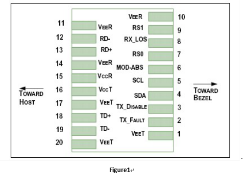
|
Pin |
Logic |
Symbol |
Name/Description |
Note |
|
1 |
|
VeeT |
Module Transmitter Ground |
Note1 |
|
2 |
LVTTL-O |
TX_Fault |
Module Transmitter Fault |
Note2 |
|
3 |
LVTTL-I |
TX_Disable |
Transmitter Disable; Turns off transmitter laser output |
Note3 |
|
4 |
LVTTL-I/O |
SDA |
2-wire Serial Interface Data Line (Same as MOD-DEF2 as defined in the INF-8074i) |
Note4 |
|
5 |
LVTTL-I/O |
SCL |
2-wire Serial Interface Clock (Same as MOD-DEF1 as defined in the INF-8074i) |
Note4 |
|
6 |
|
MOD_ABS |
Module Absent, connected to VeeT or VeeR in the module |
Note5 |
|
7 |
LVTTL-I |
RS0 |
Not used |
|
|
8 |
LVTTL-O |
RX_LOS |
Receiver Loss of Signal Indication (In FC designated as RX_LOS, in SONET designated as LOS, and in Ethernet designated at Signal Detect) |
Note2 |
|
9 |
LVTTL-I |
RS1 |
Not used |
|
|
10 |
|
VeeR |
Module Receiver Ground |
Note1 |
|
11 |
|
VeeR |
Module Receiver Ground |
Note1 |
|
12 |
CML-O |
RD- |
Receiver Inverted Data Output |
|
|
13 |
CML-O |
RD+ |
Receiver Non-Inverted Data Output |
|
|
14 |
|
VeeR |
Module Receiver Ground |
Note1 |
|
15 |
|
VccR |
Module Receiver 3.3 V Supply |
|
|
16 |
|
VccT |
Module Transmitter 3.3 V Supply |
|
|
17 |
|
VeeT |
Module Transmitter Ground |
Note1 |
|
18 |
CML-I |
TD+ |
Transmitter Non-Inverted Data Input |
|
|
19 |
CML-I |
TD- |
Transmitter Inverted Data Input |
|
|
20 |
|
VeeT |
Module Transmitter Ground |
Note1 |
Notes:
[1] The module signal ground pins, VeeR and VeeT, shall be isolated from the module case.
[2] This pin is an open collector/drain output pin and shall be pulled up with 4.7k-10kohms to Host_Vcc on the host board. Pull ups can be connected to multiple power supplies, however the host board design shall ensure that no module pin has voltage exceeding module VccT/R + 0.5 V.
[3] This pin is an open collector/drain input pin and shall be pulled up with 4.7k-10kohms to VccT in the module.
[4] See SFF-8431 4.2 2-wire Electrical Specifications .
[5] This pin shall be pulled up with 4.7k-10kohms to Host_Vcc on the host board.
Block Diagram of Transceiver
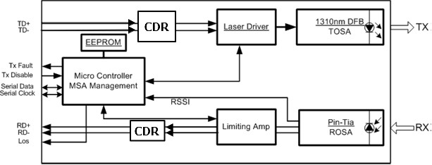
The transmitter converts 25.78Gbit/s serial PECL or CML electrical data into serial optical data compliant with the
The receiver converts 25.78Gbit/s serial optical data into serial PECL/CML electrical data. An open collector compatible Loss of Signal is provided. Rx_LOS when high indicates an optical signal level below that specified in the relevant standard. The Rx_LOS contact is an open drain/collector output and shall be pulled up to Vcc_Host in the host with a resistor in the range 4.7-10 kΩ, or with an active termination. The Rx_LOS signal is intended as a preliminary indication to the system in which the SFP+ is installed that the received signal strength is below the specified range. Such an indication typically points to non-installed cables, broken cables, or a disabled, failing or a powered off transmitter at the far end of the cable. Per the requirements of performance, internal clock and data recovery circuits (CDR) are present on electrical output of this transceiver module.
Tx input equalization control can be accessed through 2-wire serial interface at byte address 114(A2h). Tx input equalization control for 25GE is located at the upper 4 bits of byte 114 (A2h).
Rx output emphasis control can be accessed through 2-wire serial interface at byte address 115(A2h). Rx output emphasis control for 25GE is located at the upper 4 bits of byte 115 (A2h).
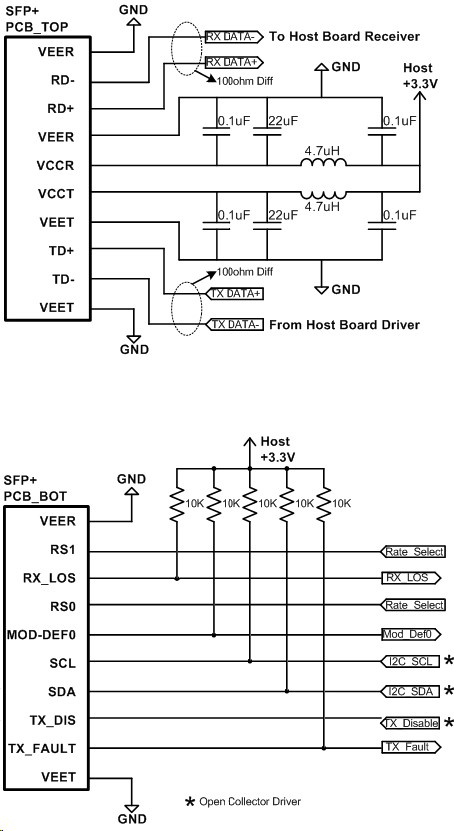
Figure3
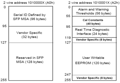
Serial ID Memory Contents(A0h)
|
Addr. |
Field Size |
Name of Field |
Hex |
Description |
|
(Bytes) |
||||
|
0 |
1 |
Identifer |
03 |
SFP |
|
1 |
1 |
Ext. Identifier |
04 |
SFP function is defined by serial ID only |
|
2 |
1 |
Connector |
07 |
LC Connector |
|
3-10 |
8 |
Transceiver |
00 00 00 00 00 00 00 00 |
10G Ethernet Compliance Codes: 10G Base-LR |
|
11 |
1 |
Encoding |
03 |
NRZ |
|
12 |
1 |
BR, Nominal |
FF |
255*100MBd |
|
13 |
1 |
Rate Identifier |
00 |
Unspecified |
|
14 |
1 |
Length (9um) km |
0A |
Transceiver transmit distance,10km |
|
15 |
1 |
Length (9um) 100m |
00 |
Transceiver transmit distance,100*100m |
|
16 |
1 |
Length (50um)10m |
00 |
Transceiver transmit distance |
|
17 |
1 |
Length (62.5um) 10m |
00 |
Transceiver transmit distance |
|
18 |
1 |
Length (Copper) |
00 |
Not compliant |
|
19 |
1 |
Length (50um OM3) |
00 |
Not compliant |
|
20-35 |
16 |
Vendor name |
48 47 20 47 45 4E 55 49 4E 45 20 20 20 20 20 20 |
“HG GENUINE” Vendor Name(ASCII) |
|
36 |
1 |
Reserved |
03 |
100GBASE-LR4 |
|
37-39 |
3 |
Vendor OUI |
00 00 00 |
|
|
40-55 |
16 |
Vendor PN |
4D 54 52 41 2D 33 45 33 |
“MTRA-3E30A”Part No.(ASCII) |
|
|
|
|
30 41 20 20 20 20 20 20 |
|
|
56-59 |
4 |
Vendor rev |
31 2E 30 20 |
“1.0” (ASCII) |
|
60-61 |
2 |
Wavelength |
05 1E |
Transceiver wavelength |
|
62 |
1 |
Reserved |
00 |
|
|
63 |
1 |
CC_BASE |
A6 |
Check code for Base ID Fields |
|
64-65 |
2 |
Options |
0A 1A |
a conventional uncooled laser Power Level 2 a conventional limiting output the transceiver has an internal retimer or CDR TX_DISABLE TX_FAULT Rx_LOS |
|
66 |
1 |
BR,MAX |
00 |
Not Specified |
|
67 |
1 |
BR,MIN |
00 |
Not Specified |
|
68-83 |
16 |
Vendor SN |
SN(Variable) |
Serial Number of transceiver(ASCII). |
|
84-91 |
8 |
Date code |
DC(Variable) |
Manufactory Date Code. |
|
92 |
1 |
Diagnostic Monitoring Type |
68 |
Digital diagnostic monitoring implemented, “internally calibrated” is implemented |
|
93 |
1 |
Enhanced Options |
B0 |
Alarm/warning flags soft TX_FAULT soft RX_LOS |
|
94 |
1 |
SFF_8472 Compliance |
08 |
Includes functionality described in Rev12.0 SFF-8472 |
|
95 |
1 |
CC_EXT |
CF(Variable) |
Check sum for Extended ID Field. |
|
96-127 |
32 |
Vendor Specific |
Read only |
Depends on customer information Filled by zero |
|
128-255 |
128 |
Reserved |
Read only |
Filled by zero |
|
Part No. |
|
Specification |
|
|
|
||||
|
Pack |
Rate |
Tx |
Pout |
Rx |
Sens. |
Top |
Reach |
Others |
|
|
MTRA-3E30A |
SFP28 |
25.78Gbps |
1310nm DFB |
-4.5~4.5 dBm |
PIN |
<-14dBm |
0~70℃ |
10km |
DDM/RoHS |
Contact Information
Wuhan Huagong Genuine Optics Technology Co., Ltd
Address: Science & Technology Region of HUST, Donghu High-Tech Zone
Wuhan, Hubei Province, 430223, China
l Tel: +86-27-87180102
l Fax: +86-27-87180220
Email: market@genuine-opto.com
Statement
HG Genuine possesses the authority for ultimate explanation of all information contained in this document, which is subject to change without prior notice. All the information was obtained in specific environments; and HG Genuine will not be responsible for verifying the products performance in customers’ operating environments, neither liable for the performance of users' products. All information contained is only for the users' reference and shall not be considered as warranted characteristics. HG Genuine will not be liable for damages arising directly or indirectly from any use of the information contained in this document.
